 ALLPCB


Why Dielectric Thickness Matters in High-Frequency Applications
Dielectric thickness refers to the distance between copper layers separated by insulating material. In high-frequency PCB design, even small variations in this dimension alter the electromagnetic field distribution. Thinner dielectrics increase capacitance per unit area, which lowers characteristic impedance for a given trace width. Conversely, thicker layers raise impedance but can increase radiation and crosstalk. The selection process must also account for dielectric material selection, because the base resin and reinforcement determine how thickness interacts with frequency-dependent properties. Proper thickness control supports consistent performance across temperature and humidity variations encountered in real-world operation.
Technical Principles Governing Dielectric Behavior
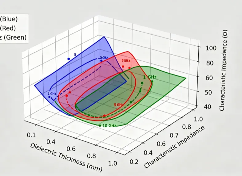
Signal propagation in high-frequency circuits depends on the interaction between the conductor and the surrounding dielectric. The characteristic impedance follows from the ratio of inductance to capacitance per unit length. Changing dielectric thickness modifies capacitance while inductance remains relatively stable for a given geometry, shifting the impedance value. Insertion loss comprises conductor loss, primarily from skin effect, and dielectric loss, which scales with the loss tangent of the material. At higher frequencies, the dielectric constant frequency dependence becomes noticeable; many materials exhibit a gradual decrease in effective permittivity as frequency rises. This shift alters phase velocity and can detune filters or matching networks if not anticipated during stack-up definition.
Dielectric loss mechanisms involve molecular friction as the electric field oscillates. Materials with lower loss tangents minimize conversion of signal energy into heat. Thickness influences the field strength within the dielectric; thinner layers concentrate the field, potentially increasing loss if the material is not optimized. In differential pairs, thickness also affects the balance between odd-mode and even-mode impedances. Engineers therefore model these effects using electromagnetic simulation before committing to fabrication. Standards such as IPC-6012E define qualification requirements that include verification of dielectric properties and layer registration to ensure the finished board meets electrical specifications.
Practical Approaches to Dielectric Thickness Selection
Begin by defining the target impedance, typically 50 ohms single-ended or 100 ohms differential, at the highest operating frequency. Use the known dielectric constant of the chosen material to calculate the required thickness for a given trace width and spacing. Account for the frequency dependence of the dielectric constant by obtaining material data at or near the application frequency rather than relying solely on datasheet values measured at 1 MHz.
Consider the cumulative effect of multiple dielectric layers in a complex stack-up. Core thickness and prepreg thickness must be chosen together to achieve the desired overall separation while maintaining symmetry for warpage control. Manufacturing tolerances on dielectric thickness, often expressed as a percentage, must be incorporated into the tolerance stack-up analysis. 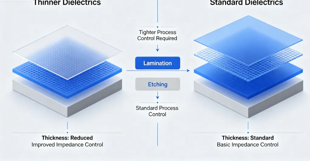
When signal loss is critical, evaluate the trade-off between thinner dielectrics that shorten the field path and materials with inherently lower loss tangents. Thermal expansion differences between copper and dielectric also influence long-term reliability; thicker dielectrics can provide mechanical buffering in some designs. Review the stack-up against IPC-A-600K acceptability criteria to confirm that thickness variations remain within limits that preserve both electrical and visual quality.
Best Practices and Verification Steps
Collaborate early with the fabricator to confirm available core and prepreg thicknesses for the selected dielectric material. Specify controlled impedance requirements on the fabrication drawing, including test frequency and acceptable tolerance. Perform post-layout simulation that incorporates the actual dielectric constant frequency dependence obtained from the material supplier.
Validate the design through test coupons included on the panel. Measure impedance and insertion loss on these coupons using time-domain reflectometry and vector network analysis. Compare results against simulation predictions to close the loop on modeling assumptions. Maintain consistent dielectric thickness across panels by specifying lamination parameters that minimize resin flow variation.
Document the rationale for each thickness choice, including frequency range, material properties, and impedance targets. This documentation supports future revisions and helps procurement teams source consistent materials. When designs push the limits of standard FR-4 type materials, evaluate high-performance laminates whose dielectric properties remain stable across the intended bandwidth.
Conclusion
Dielectric thickness selection in high-frequency PCB design integrates electrical modeling, material characterization, and manufacturing capability. Understanding the relationships among thickness, impedance, insertion loss, and dielectric constant frequency dependence enables engineers to achieve reliable signal integrity. Structured evaluation against established industry standards ensures the final board meets both performance and quality expectations. Consistent application of these principles reduces design iterations and supports predictable high-frequency operation.
FAQs
Q1: How does dielectric thickness affect insertion loss in high-frequency PCB design?
A1: Dielectric thickness influences the electromagnetic field confinement around signal traces. Thinner layers can reduce radiation loss but may increase dielectric loss if the material loss tangent is not low enough. Engineers calculate the contribution of dielectric loss to total insertion loss using the loss tangent and the effective path length through the dielectric. Proper selection balances thickness against material properties to keep overall signal attenuation within acceptable limits for the target frequency range.
Q2: What role does dielectric constant frequency dependence play in material selection?
A2: The dielectric constant of many insulating materials changes with frequency, altering effective capacitance and propagation delay. In high-frequency PCB design, using a value measured at 1 MHz for a multi-gigahertz application can lead to impedance mismatch. Material data sheets or supplier measurements at the operating frequency allow accurate modeling. Selecting materials with minimal frequency dependence simplifies stack-up design and improves broadband performance.
Q3: Why is controlled dielectric thickness important for signal integrity?
A3: Variations in dielectric thickness directly change the capacitance per unit length of a trace, shifting characteristic impedance. Even small deviations can cause reflections that degrade eye diagrams at high data rates. Fabricators control thickness through precise lamination processes, and designers specify tolerances based on simulation sensitivity analysis. Meeting these controls ensures consistent performance across production boards.
Q4: How do engineers verify dielectric thickness during high-frequency PCB manufacturing?
A4: Verification begins with incoming material inspection and continues through cross-section analysis of test coupons after lamination. Impedance testing on controlled-impedance traces provides an indirect but electrically relevant check. Standards such as IPC-6012E outline the qualification tests that confirm dielectric properties and layer registration meet specifications. Regular process monitoring maintains thickness consistency from lot to lot.
References
IPC-6012E — Qualification and Performance Specification for Rigid Printed Boards. IPC, 2017
IPC-A-600K — Acceptability of Printed Boards. IPC, 2020
JEDEC J-STD-020E — Moisture/Reflow Sensitivity Classification. JEDEC, 2014





