ALLPCB


Introduction
Printed circuit board design requires careful attention to thermal management to support long-term component performance. Thermal relief connections limit excessive heat flow from component pads into large copper planes during soldering operations. This controlled heat transfer helps prevent damage to sensitive parts and maintains structural integrity of the board. Engineers who incorporate effective thermal relief strategies early in the layout process often observe improved assembly yields and reduced field failures. Such practices contribute directly to extending component life with thermal design approaches that balance electrical and thermal requirements.
Understanding PCB Thermal Relief and Its Importance
PCB thermal relief refers to specialized pad patterns that connect component leads to copper planes while restricting direct thermal paths. These patterns typically use narrow spokes or bridges that allow solder to flow properly yet reduce heat sinking effects. In high-density boards, inadequate relief can cause uneven heating that stresses joints and accelerates material fatigue. The reliability impact thermal relief produces becomes evident through lower rates of delamination and cracking over repeated thermal cycles. Industry professionals recognize that thoughtful thermal relief implementation supports consistent manufacturing outcomes across various board thicknesses and layer counts. 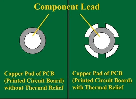
Technical Mechanisms of Thermal Relief in PCBs
Thermal relief functions by creating a partial thermal barrier between the pad and surrounding copper areas. During reflow soldering, this barrier allows localized heat buildup sufficient for solder melting without drawing excessive energy away from the joint. Reduced heat transfer minimizes temperature gradients that otherwise lead to board warpage or component package cracking. Over the operational life of an assembly, these same mechanisms help lower cumulative thermal stress that contributes to solder joint fatigue. Engineers analyze trace widths, spoke dimensions, and plane coverage to optimize the balance between electrical conductivity and thermal isolation. Proper execution of these principles supports thermal stress reduction PCB designs that maintain performance under varying environmental loads.
Related Reading: Copper Pour and Thermal Relief: A Guide to Preventing Soldering Issues
Best Practices for Implementing Thermal Relief
Design teams begin by evaluating component power dissipation and expected soldering profiles before selecting relief patterns. Standard practice involves using four-spoke configurations for most through-hole and surface-mount pads attached to planes. Adjustments to spoke width and length allow fine-tuning of thermal resistance while preserving adequate current-carrying capacity. Simulation tools help verify that relief features do not introduce excessive voltage drop or inductance in high-speed circuits. Documentation of these choices during layout review ensures consistent application across multiple board revisions. Following established guidelines from IPC-6012E helps maintain qualification compliance for rigid printed boards throughout the design cycle.
Troubleshooting Thermal Stress Issues in PCB Assemblies
When thermal stress symptoms appear, such as lifted pads or cracked components, engineers first inspect relief geometry against original specifications. Common causes include overly wide spokes that defeat the intended isolation or insufficient plane clearance around pads. Rework procedures may involve adding temporary heat shields or adjusting reflow oven profiles to compensate for existing board features. Post-assembly inspection under IPC-A-600K criteria allows identification of acceptable versus nonconforming thermal relief implementations. Iterative testing of revised layouts confirms that modifications achieve the desired reduction in component stress without compromising electrical performance.
Related Reading: Thermal Stress Testing: Validating PCB Reliability Under Extreme Conditions
Conclusion
Effective thermal relief design directly influences both immediate manufacturing success and long-term component reliability. By managing heat flow during soldering and subsequent operation, these features reduce mechanical stress that shortens product life. Structured application of relief patterns, combined with adherence to recognized standards, provides engineers with repeatable methods for achieving consistent results. Continued attention to these details throughout the development process supports higher overall system dependability.
FAQs
Q1: How does PCB thermal relief affect component lifespan?
A1: Proper thermal relief limits heat transfer to component packages during soldering and reduces ongoing thermal cycling stress. This controlled environment decreases the rate of material fatigue and joint degradation, thereby extending component life with thermal design practices that maintain electrical performance.
Q2: What is the reliability impact of thermal relief in PCB layouts?
A2: Thermal relief patterns minimize temperature gradients that cause warpage and solder joint cracking. When implemented according to established guidelines, these features lower failure rates in both assembly and field operation, improving overall board reliability.
Q3: Can thermal stress reduction PCB techniques improve assembly yields?
A3: Yes, optimized relief connections promote even solder flow and prevent cold joints or component damage. Consistent application of these techniques results in fewer defects and higher first-pass yields during manufacturing.
Q4: Why should designers consider thermal relief early in the PCB process?
A4: Early integration allows simulation and adjustment of relief parameters before fabrication. This proactive approach avoids costly redesigns and ensures the final assembly meets both thermal and electrical requirements.
References
IPC-6012E — Qualification and Performance Specification for Rigid Printed Boards. IPC, 2017
IPC-A-600K — Acceptability of Printed Boards. IPC, 2020
JEDEC J-STD-020E — Moisture/Reflow Sensitivity Classification. JEDEC, 2014