 ALLPCB


Printed circuit boards (PCBs) are the backbone of modern electronics, powering everything from smartphones to aerospace systems. However, their reliability under extreme conditions—such as high temperatures, rapid thermal cycling, or harsh environments—can make or break a product's success. Thermal stress testing is a critical process to ensure PCBs can withstand these challenges, preventing costly failures and ensuring long-term performance. In this blog, we explore the importance of thermal stress testing, its key methods, and how it validates PCB reliability for demanding applications.
Whether you're designing for consumer electronics or mission-critical systems, understanding thermal stress testing empowers you to build robust, dependable PCBs. Let's dive into the essentials of this process and uncover practical insights for engineers.
Why Thermal Stress Testing Matters for PCB Reliability
PCBs operate in diverse environments, from the heat of an automotive engine bay to the freezing altitudes of aerospace applications. Without rigorous testing, thermal stresses can lead to failures like solder joint fractures, via cracks, or material delamination. According to industry standards like IPC-6012, thermal reliability is non-negotiable for high-performance HDI PCBs, especially in Class 3 applications for medical and military systems, where failure risks human safety.
Thermal stress testing simulates real-world conditions to identify weaknesses before mass production. By exposing PCBs to extreme temperatures and rapid transitions, engineers can pinpoint failure modes, optimize designs, and ensure compliance with standards like JEDEC and MIL-STD. For example, a study found that thermal cycling between -40°C and +125°C can reduce solder joint life by up to 50% if not properly managed. This data underscores why proactive testing is essential for reliability.
Key Thermal Stress Testing Methods
Thermal stress testing encompasses several methods, each designed to evaluate specific aspects of PCB reliability. Below, we outline the most common techniques and their applications.
Thermal Cycling Testing
Thermal cycling involves subjecting PCBs to repeated temperature fluctuations, typically between -65°C and +125°C, over hundreds or thousands of cycles. This method simulates the thermal stresses a PCB experiences during its operational life, such as powering on and off in a consumer device. The goal is to assess fatigue in solder joints, vias, and substrate materials caused by differences in coefficients of thermal expansion (CTE).
For instance, a PCB with a FR-4 substrate (CTE ~14 ppm/°C) and copper traces (CTE ~17 ppm/°C) may experience stress at solder joints during temperature swings. Testing might involve 1,000 cycles with a transition rate of 10°C per minute, as per JEDEC JESD22-A104. Failures like micro-cracks in solder joints or delamination are detected through electrical testing and microsection analysis post-cycling.
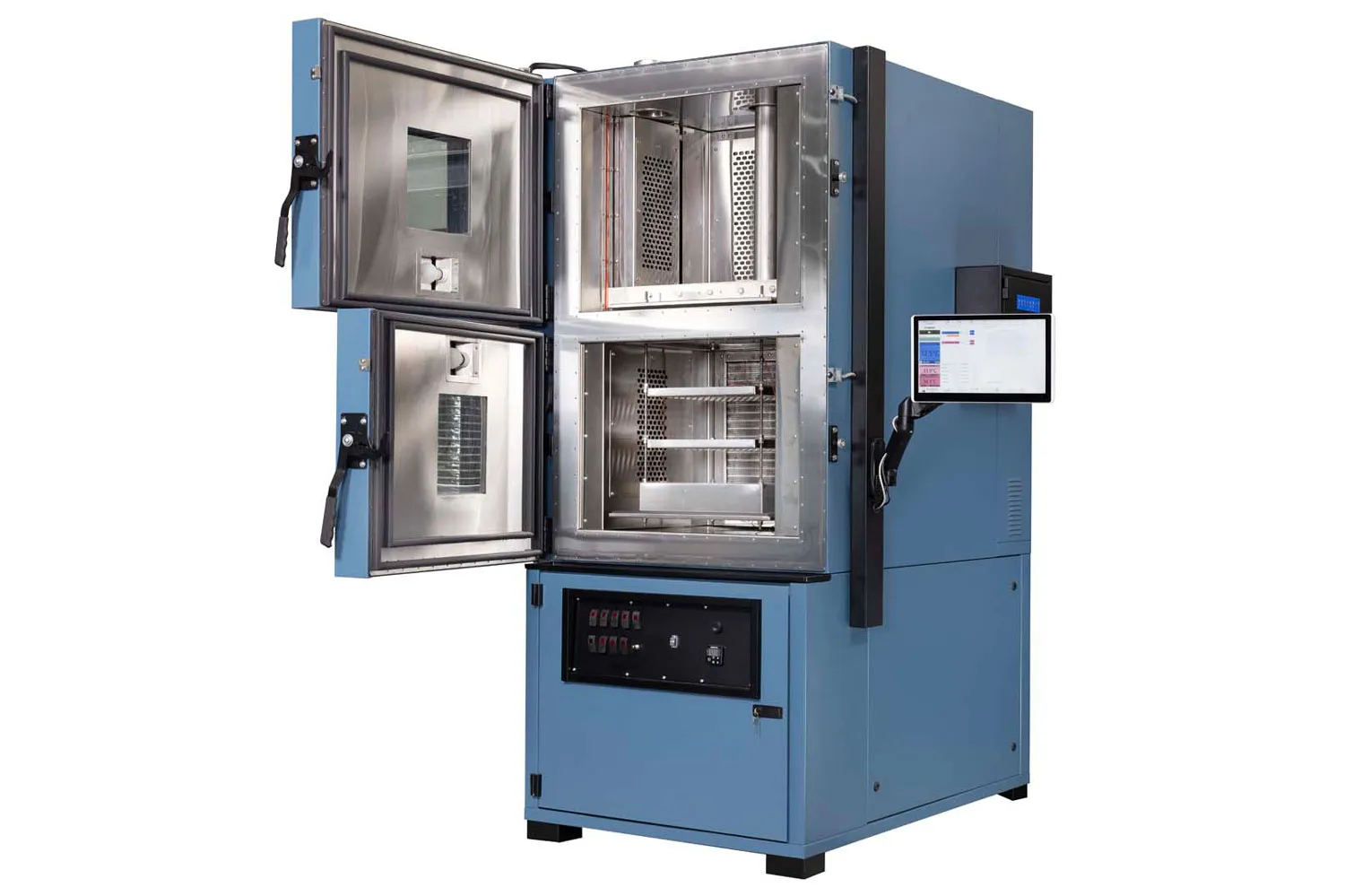
Thermal Shock Testing
Unlike thermal cycling's gradual transitions, thermal shock testing exposes PCBs to rapid temperature changes, often exceeding 15°C per minute. This method mimics extreme scenarios, such as a PCB in a satellite transitioning from sunlight to shadow. Tests are conducted in dual-chamber systems or liquid baths, with temperatures ranging from -55°C to +150°C, per standards like IPC-TM-650 Method 2.6.7.
Thermal shock is particularly harsh on plated-through holes (PTHs). A 2017 IEEE study found that rapid transitions from -40°C to +160°C increased PTH failure rates by 30% due to CTE mismatches. Microsectioning after testing reveals issues like barrel cracking or separation, ensuring PTH integrity before assembly.
Burn-In Testing
Burn-in testing subjects PCBs to elevated temperatures (e.g., 125°C) and electrical stress for extended periods, typically 24–168 hours. This method identifies latent defects, such as weak components or manufacturing flaws, that might cause early failures. Burn-in is common for high-reliability applications, like aerospace, where a single failure could be catastrophic.
For example, a burn-in test might apply 500VDC across a PCB's conductors while maintaining 105°C to simulate worst-case operating conditions. Continuous monitoring detects anomalies like insulation breakdown or component degradation, ensuring only robust PCBs reach the field.
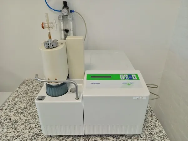
Coefficient of Thermal Expansion (CTE) Testing
CTE testing measures how PCB materials expand or contract with temperature changes, using tools like Thermal Mechanical Analysis (TMA). This is critical for multilayer PCBs, where mismatched CTEs between laminate, copper, and solder can cause stress. A typical test heats a 6.35mm x 6.35mm sample from 105°C to 250°C at 10°C/min, recording expansion to ensure it stays within acceptable limits (e.g., <50 ppm/°C post-glass transition).
High CTE mismatches can lead to via fractures or delamination. For instance, ceramic substrates (CTE ~7 ppm/°C) are preferred for high-temperature applications to minimize stress, unlike FR-4, which may deform above 150°C.
Common Failure Modes Uncovered by Thermal Stress Testing
Thermal stress testing reveals several failure modes that compromise PCB reliability. Understanding these helps engineers design more robust boards.
- Solder Joint Fatigue: Repeated thermal cycling causes stress concentration at solder ball interfaces, leading to micro-cracks or open circuits. A 2022 study noted that lead-free SAC305 solder joints failed after 1,500 cycles between -40°C and +125°C due to fatigue.
- Via and PTH Cracking: CTE mismatches between copper plating and substrate materials can fracture vias or PTHs, especially under thermal shock. High-aspect-ratio vias are particularly vulnerable, with failure rates increasing by 20% in rapid temperature shifts.
- Delamination: Extreme heat can cause separation between laminate layers, weakening the PCB's structural integrity. This is common in low-Tg substrates exposed to temperatures above 150°C.
- Component Failure: Thermally induced stresses, like electromigration in ICs, can cause immediate or long-term component failures, reducing PCB lifespan.
By identifying these issues early, engineers can adjust materials, layouts, or manufacturing processes to enhance reliability.
Industry Standards for Thermal Stress Testing
Adhering to industry standards ensures consistent, reliable testing outcomes. Key standards include:
- IPC-TM-650 Method 2.6.8: Specifies thermal stress testing for PTHs using a solder float method at 288°C for 10 seconds, followed by microsection analysis to check for cracks or separations.
- JEDEC JESD22-A104: Governs thermal cycling tests, defining temperature ranges (-65°C to +150°C), cycle counts, and transition rates for semiconductor packages and PCBs.
- MIL-STD-202: Outlines environmental stress tests, including thermal shock and humidity, for military-grade PCBs, ensuring durability in extreme conditions.
- IEC 60068: Covers environmental testing, including thermal cycling and shock, with specific protocols for heat, vibration, and humidity resistance.
Compliance with these standards ensures PCBs meet performance expectations in their intended applications, from consumer gadgets to critical infrastructure.
Practical Tips for Designing Thermally Reliable PCBs
To maximize PCB reliability under thermal stress, consider these design strategies:
1. Match CTE Values: Select materials with similar CTEs for substrates, conductors, and solder. For example, using a high-Tg FR-4 (Tg >170°C) reduces stress compared to standard FR-4 (Tg ~130°C).
2. Optimize Via Design: Use low-aspect-ratio vias and ensure proper copper plating thickness (e.g., 25 µm) to minimize cracking during thermal shock.
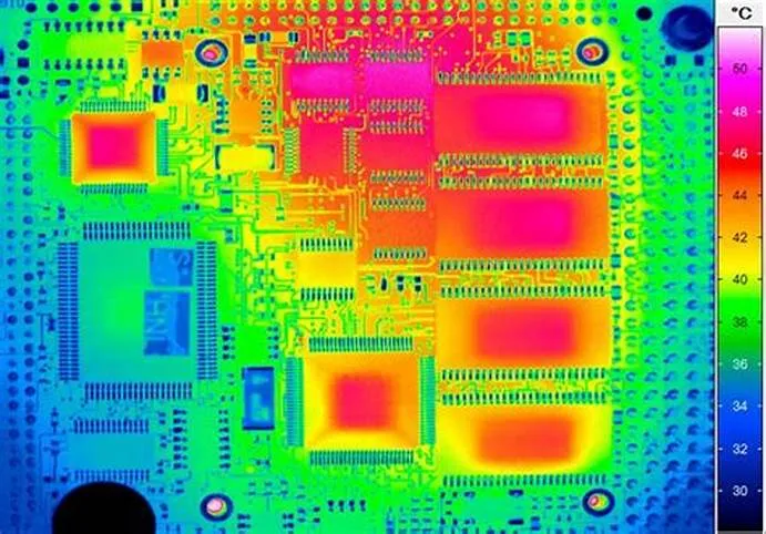
3. Enhance Thermal Management: Incorporate thermal vias, heat sinks, or metal-core substrates to dissipate heat evenly, preventing hotspots that exacerbate stress.
4. Simulate Thermal Performance: Use probabilistic modeling tools like Cadence OrCAD to predict thermal hotspots and stress points before prototyping.
5. Test Early and Often: Conduct thermal stress tests on prototype coupons to catch issues before full-scale production, reducing costly recalls.
These practices, grounded in data and standards, help engineers build PCBs that withstand extreme conditions.
How ALLPCB Supports Thermal Stress Testing
At ALLPCB, we understand the critical role thermal stress testing plays in delivering reliable PCBs. Our advanced manufacturing capabilities and quick-turn prototyping services enable engineers to test and refine designs rapidly, ensuring robustness under extreme conditions. With global logistics and state-of-the-art facilities, we provide high-quality PCBs that meet stringent standards like IPC-6012 and JEDEC, supporting applications from consumer electronics to aerospace. Partner with us to streamline your prototyping and production, confident that your PCBs are built to endure the toughest thermal challenges.
Conclusion: Building Reliable PCBs for the Future
Thermal stress testing is more than a quality assurance step—it's a cornerstone of PCB reliability in demanding environments. Byyour designs to life with confidence.


