ALLPCB


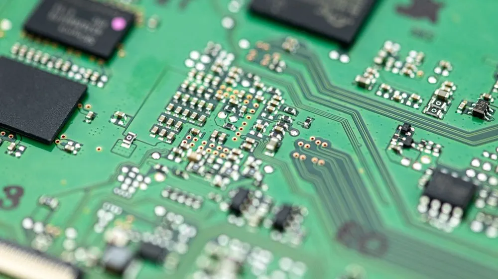
In the world of PCB design and assembly, achieving reliable soldering and effective heat dissipation can be a challenge. Two critical elements—copper pour and thermal relief—play a significant role in ensuring your printed circuit board (PCB) performs well during manufacturing and operation. But how do copper pour and thermal relief help prevent soldering issues in PCB assembly? Simply put, copper pour helps with heat dissipation and electrical connectivity, while thermal relief ensures proper soldering by managing heat flow during the process. In this comprehensive guide, we’ll dive deep into these concepts, explore their importance in preventing soldering issues, and provide practical tips for optimizing your PCB design for better heat dissipation and assembly outcomes.
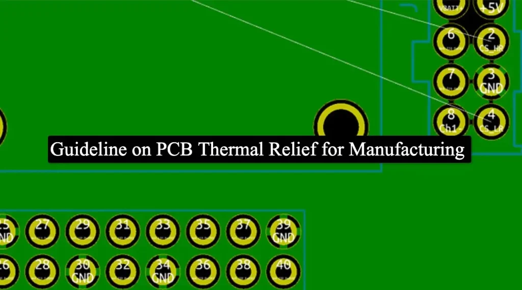
What Are Copper Pour and Thermal Relief in PCB Design?
Before we explore their impact on soldering and heat dissipation, let’s define copper pour and thermal relief. These terms are essential for anyone involved in PCB assembly and design.
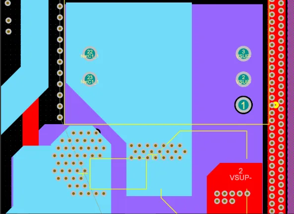
Copper Pour: A copper pour refers to a large area of copper on a PCB layer, often used to create ground or power planes. It serves multiple purposes, including providing a low-impedance path for electrical signals, reducing noise, and aiding in heat dissipation. By spreading heat across a larger surface area, copper pours help prevent overheating of components during operation.
Thermal Relief: Thermal relief is a design technique used to manage heat during soldering. It involves creating a pattern of copper connections—often in the form of spokes—between a component pad and a larger copper plane (like a ground or power plane). This design limits the heat flow from the pad to the plane, ensuring that the soldering iron or reflow process can adequately heat the pad without being overwhelmed by the heat-sinking effect of the copper plane.
Why Soldering Issues Occur in PCB Assembly
Soldering issues are a common problem in PCB assembly, often leading to weak joints, component damage, or complete failure of the board. Understanding why these issues happen is the first step to preventing them.
One major cause of soldering problems is uneven heat distribution during the soldering process. When a component pad is directly connected to a large copper plane without thermal relief, the copper acts as a heat sink, pulling heat away from the pad. This can result in insufficient heating of the solder joint, leading to cold solder joints or incomplete bonding. For example, during reflow soldering, a pad without thermal relief might not reach the required temperature of around 230°C for proper solder melting, while surrounding areas overheat.
Another issue is thermal stress. Large copper areas can cause rapid heat dissipation, leading to uneven expansion and contraction of the PCB material. This stress can damage components or crack solder joints over time, especially in high-power applications where heat cycles are frequent.
By incorporating copper pour and thermal relief into your design, you can address these challenges and ensure reliable soldering in PCB assembly.
The Role of Copper Pour in Heat Dissipation and Soldering
Copper pour is a powerful tool for managing heat in a PCB. By creating large areas of copper, you provide a path for heat to spread out, reducing the risk of hot spots that can damage components. For instance, in high-current applications, components like power transistors can generate significant heat—sometimes exceeding 100°C. A well-designed copper pour can lower the temperature by distributing this heat across the board.
However, while copper pour excels at heat dissipation during operation, it can create challenges during soldering. A large copper area absorbs and dissipates heat quickly, making it difficult to maintain the high temperatures needed for soldering (typically 260°C to 300°C for lead-free solder). Without proper design considerations, this can lead to incomplete solder joints or prolonged soldering times, which might damage sensitive components.
This is where balancing copper pour with other design techniques becomes essential. Limiting the size of copper pour near soldering pads or integrating thermal relief patterns can help maintain the benefits of heat dissipation while ensuring successful soldering.
How Thermal Relief Prevents Soldering Issues
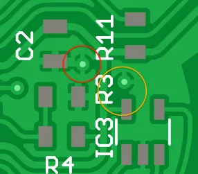
Thermal relief is specifically designed to tackle soldering challenges associated with large copper areas. By adding a thermal relief pattern—typically a set of thin copper spokes connecting the pad to the copper plane—you restrict the heat flow away from the pad during soldering. This allows the pad to reach the necessary temperature for a strong solder joint without excessive heat loss to the surrounding copper.
For example, a typical thermal relief design might feature four spokes, each 0.3 mm wide, connecting a 1.5 mm pad to a ground plane. This configuration ensures electrical connectivity while limiting heat dissipation during soldering. Studies suggest that thermal relief can reduce the time to reach soldering temperature by up to 50%, significantly improving assembly outcomes.
Thermal relief also helps reduce thermal stress on components. By controlling heat flow, it prevents rapid temperature changes that could cause mechanical stress or damage to delicate parts like ceramic capacitors or fine-pitch ICs.
Best Practices for Using Copper Pour and Thermal Relief in PCB Design
Now that we understand the importance of copper pour and thermal relief, let’s explore actionable tips to incorporate them into your PCB design for optimal heat dissipation and soldering results.
1. Optimize Copper Pour Placement
Place copper pours strategically to maximize heat dissipation while minimizing interference with soldering. For high-power components, use thicker copper layers (e.g., 2 oz/ft2 or higher) to enhance heat spreading. Keep copper pours away from small or densely packed pads to avoid excessive heat sinking during assembly.
2. Design Effective Thermal Relief Patterns
When designing thermal relief, balance electrical connectivity with heat management. Use 3 to 4 spokes per pad, with a width of 0.2 to 0.5 mm, depending on the current requirements. Ensure the spoke length is sufficient to limit heat flow—typically 0.5 mm or more. Most PCB design software allows you to set these parameters automatically for consistency across your board.
3. Consider Component Placement
Place heat-generating components near copper pour areas to leverage their heat dissipation capabilities. However, ensure that pads for soldering have thermal relief to prevent heat loss during assembly. For instance, a power MOSFET generating 5W of heat can benefit from a nearby copper pour, but its pads should feature thermal relief for reliable soldering.
4. Use Thermal Vias for Multilayer Boards
In multilayer PCBs, thermal vias can complement copper pours by transferring heat between layers. Place an array of vias (e.g., 0.3 mm diameter, spaced 1 mm apart) under high-heat components to connect to internal copper planes. This enhances overall heat dissipation without affecting soldering performance when combined with thermal relief.
5. Test and Iterate Your Design
Always simulate your PCB design for thermal performance using tools like thermal analysis software. Check for hot spots or areas where heat dissipation might be insufficient. After manufacturing, inspect solder joints for quality to ensure that thermal relief patterns are effective. Adjust your design as needed based on real-world testing.
Common Mistakes to Avoid with Copper Pour and Thermal Relief
Even with the best intentions, mistakes in implementing copper pour and thermal relief can lead to soldering issues or poor heat dissipation. Here are some pitfalls to watch out for:
Overusing Copper Pour: Covering too much of the PCB with copper pour can make soldering nearly impossible without thermal relief. Limit copper pour to areas where it’s needed for heat dissipation or electrical grounding.
Inadequate Thermal Relief: Designing thermal relief with spokes that are too wide or too few can fail to restrict heat flow, leading to cold solder joints. Stick to recommended dimensions for spoke width and count.
Ignoring Component Heat Needs: Failing to account for the heat output of components can result in insufficient copper pour or vias, causing overheating during operation. Always match heat dissipation solutions to component specifications.
Neglecting Multilayer Heat Paths: In multilayer boards, heat can build up in internal layers if not addressed with vias or proper copper distribution. Ensure heat paths are designed across all layers.
The Impact of Copper Pour and Thermal Relief on PCB Assembly Costs
While copper pour and thermal relief are essential for performance, they can influence PCB assembly costs. Larger copper areas may require more material, especially if thicker copper layers are used for heat dissipation. However, the cost is often offset by the reduced risk of soldering defects and component failures, which can lead to expensive rework or recalls.
Thermal relief, on the other hand, typically doesn’t add significant cost since it’s a design feature rather than a material addition. In fact, it can save money by improving soldering yield during assembly. For instance, a well-designed thermal relief pattern can reduce soldering defects by up to 30%, lowering the need for manual touch-ups.
Conclusion: Mastering Copper Pour and Thermal Relief for Better PCBs
Incorporating copper pour and thermal relief into your PCB design is a proven way to prevent soldering issues and enhance heat dissipation. Copper pour helps manage heat during operation by spreading it across the board, while thermal relief ensures reliable soldering by controlling heat flow during assembly. By following best practices—such as optimizing copper placement, designing effective thermal relief patterns, and avoiding common mistakes—you can create PCBs that perform reliably in both manufacturing and real-world use.
Whether you’re designing a simple single-layer board or a complex multilayer PCB, these techniques are essential for achieving high-quality results. With careful planning and attention to detail, you can tackle soldering challenges head-on and ensure your PCB assembly process is smooth and efficient. Remember, a well-designed PCB not only saves time and money but also delivers long-term reliability for your electronic projects.