 ALLPCB


Multilayer printed circuit boards require precise lamination to bond copper layers and insulating materials into a stable structure. Two primary approaches dominate fabrication: traditional lamination and sequential lamination. Engineers evaluating these methods focus on layer count, via technology, signal integrity requirements, and overall board complexity. The choice directly influences manufacturing yield, thermal performance, and the ability to support high-density interconnect features. Understanding the distinctions helps design teams align fabrication processes with application demands.
What Is Traditional Lamination in PCB Fabrication
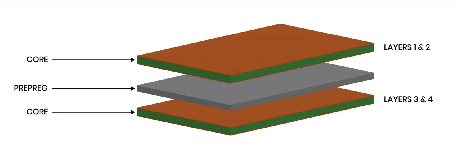
Traditional lamination assembles all layers of a multilayer PCB in a single pressing cycle. Core materials, prepreg sheets, and copper foils are stacked according to the design and subjected to heat and pressure simultaneously. This method suits standard multilayer boards where through-hole vias connect all layers. It remains common for applications that do not require buried or blind vias spanning only specific layer groups. The process aligns with established qualification requirements outlined in IPC-6012E.
What Is Sequential Lamination in PCB Fabrication
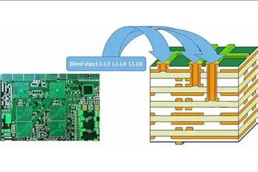
Sequential lamination builds the board in stages by laminating subsets of layers multiple times. After the first lamination cycle, additional layers are added, drilled for microvias if needed, and laminated again. This iterative approach enables the creation of HDI structures with finer lines, smaller vias, and higher layer counts without excessive stress on inner layers. Sequential lamination supports designs where different via types connect specific layer pairs rather than traversing the entire stack. It addresses the limitations of single-cycle pressing when feature sizes shrink below conventional thresholds.
Related Reading: The Engineer's Guide to Sequential Lamination: Materials, Processes, and Best Practices
Technical Principles of the Two Lamination Techniques
In traditional lamination the entire stack experiences uniform temperature and pressure profiles during one cycle. Resin flow must fill all voids across the full thickness while maintaining registration accuracy for all drilled holes. Misalignment risks increase with higher layer counts because inner layers undergo the full thermal excursion. Sequential lamination reduces this exposure by processing thinner sub-stacks first. Each subsequent cycle laminates new layers onto an already cured core, allowing independent via formation between layer groups. Microvia drilling occurs between cycles, enabling stacked or staggered via structures that improve routing density. Both techniques must satisfy acceptability criteria described in IPC-A-600K for final board quality.
Comparison of PCB Fabrication Outcomes
Traditional lamination generally offers shorter cycle times and lower tooling complexity for boards up to eight or ten layers. It produces reliable through-hole connectivity across the full thickness when via aspect ratios remain within standard limits. Sequential lamination extends processing time and cost but delivers superior control over local via formation and reduced warpage in high-layer-count or asymmetric constructions. Signal integrity benefits arise from shorter via stubs possible with blind and buried vias created during intermediate steps. Thermal management considerations differ because sequential builds can incorporate varied dielectric thicknesses between layer pairs.
Best Practices for Selecting a Lamination Method
Design teams begin by reviewing layer count, via requirements, and minimum feature sizes against target board thickness. Boards with predominantly through-hole vias and moderate density typically proceed with traditional lamination to minimize steps. When microvias or layer-specific connectivity become necessary, sequential lamination provides the required flexibility while maintaining compliance with material and process standards. Early collaboration between design and fabrication engineers helps identify registration tolerances and thermal profiles that affect yield. Material selection must account for glass transition temperature and resin flow characteristics to prevent defects during either process.
Related Reading: Materials Matter: Selecting the Best Laminates for Sequential Lamination in HDI PCBs
Practical Guidance for Engineers
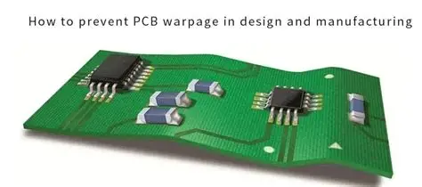
Engineers should evaluate the full stackup for symmetry to reduce warpage risk regardless of lamination approach. Sequential lamination benefits complex HDI designs but requires careful planning of drill sequences and copper balancing between cycles. Traditional lamination remains advantageous when cost and lead time constraints dominate and via technology stays conventional. Verification of final board dimensions and via integrity follows the same acceptance protocols in both cases.
Conclusion
The decision between sequential lamination and traditional lamination hinges on design complexity, via architecture, and production economics. Traditional lamination delivers efficient results for many multilayer applications, while sequential lamination enables advanced HDI features through staged processing. Engineers achieve optimal outcomes by matching the method to specific electrical and mechanical requirements while adhering to recognized industry specifications.
FAQs
Q1: What distinguishes sequential lamination from traditional lamination PCB processes?
A1: Sequential lamination builds multilayer boards through multiple pressing cycles that add layers progressively and allow intermediate microvia formation. Traditional lamination completes the entire stack in one cycle. The distinction affects via types, routing density, and overall fabrication time for multilayer PCB manufacturing.
Q2: When should designers choose sequential lamination versus traditional lamination for HDI PCB vs standard PCB projects?
A2: Designers select sequential lamination when blind or buried microvias and fine-line features exceed the capabilities of single-cycle pressing. Traditional lamination suffices for standard multilayer boards relying on through-hole vias. Evaluation of layer count and interconnect density guides the choice in PCB fabrication methods comparison.
Q3: How do lamination techniques influence reliability in multilayer PCB manufacturing?
A3: Both methods produce reliable boards when process controls maintain registration and resin flow within specified limits. Sequential lamination can reduce inner-layer stress in high-count stacks, while traditional lamination offers simplicity for conventional designs. Compliance with IPC-6012E supports consistent performance across applications.
Q4: What factors affect cost and lead time in sequential lamination vs traditional lamination PCB fabrication?
A4: Sequential lamination increases cycle count and therefore extends lead time and cost for complex HDI constructions. Traditional lamination reduces steps for boards without advanced via requirements. Early stackup review helps balance performance needs against manufacturing constraints.
References
IPC-6012E — Qualification and Performance Specification for Rigid Printed Boards. IPC, 2017
IPC-A-600K — Acceptability of Printed Boards. IPC, 2020





