 ALLPCB


Molded interconnect device PCBs combine injection-molded plastic substrates with integrated conductive traces to create three-dimensional circuit carriers. This approach supports compact electronic assemblies where traditional flat boards reach their limits in size or shape. Engineers adopt these structures to reduce part count, shorten assembly paths, and achieve higher component density within constrained volumes. The technology suits applications that demand complex geometries while maintaining electrical performance. Design teams must address both planar and non-planar layout constraints from the earliest concept stage.
Understanding High-Density Interconnect Design in MID PCBs
High-density interconnect design in molded interconnect devices extends conventional PCB principles into three dimensions. Traces follow curved or angled surfaces created during the molding process, which introduces new variables for spacing, routing, and thermal expansion. The resulting layouts allow circuits to occupy surfaces that would otherwise remain unused. This capability proves valuable when overall product dimensions must shrink without sacrificing functionality. Engineers evaluate mechanical stress on traces early because molded substrates can exhibit different coefficients of thermal expansion than standard laminates.
Technical Principles of 3D PCB Layout Guidelines
Three-dimensional PCB layout guidelines begin with substrate geometry definition. Designers establish minimum bend radii and wall thicknesses that preserve trace integrity after molding. Trace routing must account for draft angles and parting lines that affect conductor continuity. Via placement shifts from simple through-holes to laser-drilled or molded-in connections that align with the final three-dimensional form. Thermal management considerations include heat flow paths along the molded surfaces rather than solely through planar copper planes. Material selection influences both electrical and mechanical behavior, requiring verification against expected operating temperatures and humidity levels.

Signal paths in these structures experience varying dielectric environments as traces transition between flat and contoured regions. Controlled impedance becomes essential when high-speed signals travel across these transitions. Engineers model trace width, thickness, and surrounding plastic thickness to maintain target impedance values. Return paths must remain continuous despite changes in substrate orientation. Ground planes or reference conductors often follow the same three-dimensional contours to minimize loop inductance.
Related Reading: HDI PCB: A Beginner's Guide to High Density Interconnect
Trace Impedance Control MID and Signal Integrity MID Considerations
Trace impedance control MID requires precise definition of conductor geometry and dielectric properties throughout the molded part. Target impedance values are set early and verified through electromagnetic simulation that incorporates the actual three-dimensional shape. Variations in plastic thickness or trace depth directly affect characteristic impedance, so molding tolerances receive close attention. Differential pairs demand matched lengths and consistent spacing even when routed around corners or across multiple planes. Post-molding warpage can alter these dimensions, making process capability studies necessary before finalizing layouts.
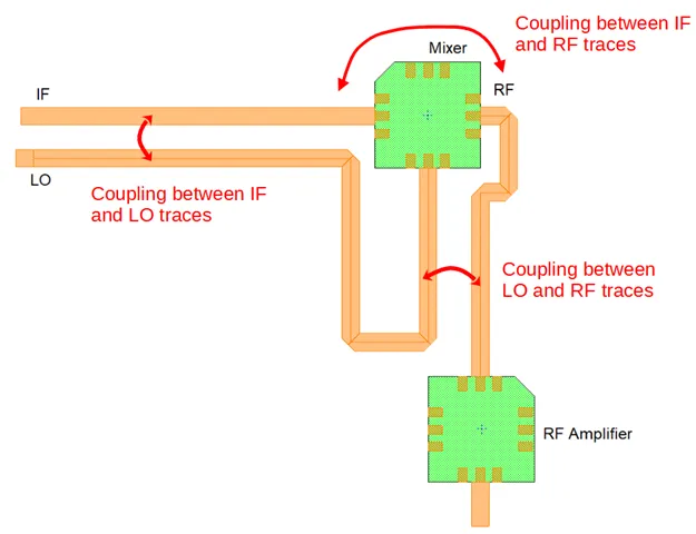
Signal integrity MID analysis extends beyond simple reflection checks. Crosstalk between adjacent traces increases when conductors run parallel on non-coplanar surfaces. Engineers evaluate both near-end and far-end coupling while considering the molded material's dielectric constant and loss tangent. Via transitions and connector interfaces introduce additional discontinuities that require compensation through localized trace adjustments. Power distribution networks must maintain low impedance across the three-dimensional structure to support stable voltage delivery to all components.
Practical Solutions and Best Practices for MID PCB Design Rules
Design teams begin with a detailed mechanical model that defines all surfaces available for circuitry. Minimum trace widths and clearances follow established PCB design rules but receive additional margins to accommodate molding process variation. Layer stack-up planning accounts for the single-sided or double-sided nature typical of many molded parts. Component placement prioritizes locations that minimize mechanical stress during subsequent assembly steps. Test points and fiducials are positioned on accessible surfaces after molding.
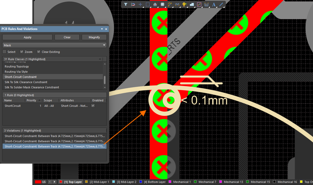
Design rule checks incorporate three-dimensional clearance verification rather than two-dimensional only. Automated tools flag violations where traces approach molded features such as ribs or bosses. Thermal simulation confirms that heat-generating components do not exceed material limits when mounted on the plastic substrate. Prototype builds undergo electrical testing at multiple stages to validate impedance and signal integrity before committing to production tooling.
Manufacturing and Quality Considerations
Molding process parameters influence final electrical performance, so designers collaborate with manufacturing engineers on material flow and cooling rates. Post-mold annealing or stress-relief steps may be required to control dimensional stability. Inspection methods include both visual examination and electrical probing adapted for three-dimensional shapes. Standards such as IPC-2221 provide foundational guidance on design considerations that apply to these non-traditional substrates. Additional verification against IPC-6012 helps confirm that finished parts meet qualification expectations for rigid printed boards.
Related Reading: Tackling Challenging Geometries: Solder Paste Dispensing on 3D MIDs
Conclusion
High-density molded interconnect device PCBs offer significant advantages in miniaturization and integration when design rules are applied systematically. Attention to three-dimensional geometry, impedance control, and signal integrity ensures reliable performance. Early collaboration between electrical, mechanical, and manufacturing teams reduces iteration cycles. Adherence to recognized standards supports consistent quality across development and production phases.
FAQs
Q1: What are the primary MID PCB design rules for high-density applications?
A1: Engineers establish minimum trace widths, clearances, and bend radii that account for molding tolerances and three-dimensional routing. These rules extend conventional PCB guidelines to curved surfaces while maintaining electrical performance. Early verification through simulation and prototype testing confirms compliance before tooling investment.
Q2: How does high-density interconnect design differ in molded interconnect devices?
A2: High-density interconnect design in MID PCBs incorporates non-planar trace routing and variable dielectric thicknesses created during molding. Engineers must manage impedance and crosstalk across transitions between flat and contoured regions. This approach enables greater component density within complex product housings compared with flat substrates.
Q3: Why is trace impedance control MID critical for signal integrity MID?
A3: Trace impedance control MID ensures consistent characteristic impedance along conductors that follow three-dimensional paths. Variations caused by substrate geometry or material thickness can degrade signal quality through reflections or increased crosstalk. Proper modeling and process control preserve signal integrity across the molded structure.
Q4: What 3D PCB layout guidelines help prevent common MID issues?
A4: Three-dimensional PCB layout guidelines emphasize continuous return paths, matched lengths for differential signals, and adequate clearances around molded features. Thermal and mechanical simulations identify potential stress points before production. These practices reduce warpage effects and maintain electrical performance after molding.
References
IPC-2221B — Generic Standard on Printed Board Design. IPC, 2012
IPC-6012E — Qualification and Performance Specification for Rigid Printed Boards. IPC, 2017
JEDEC J-STD-020E — Moisture/Reflow Sensitivity Classification. JEDEC, 2014





