ALLPCB


In the fast-evolving world of electronics, creating compact and efficient devices often means working with complex shapes and designs. One of the biggest challenges is applying solder paste on 3D Molded Interconnect Devices (3D-MIDs), where traditional methods fall short due to non-flat surfaces and intricate geometries. So, how do manufacturers achieve precise solder paste dispensing on 3D-MIDs? The answer lies in advanced techniques like selective dispensing and specialized 3D soldering methods tailored for complex structures. In this blog, we’ll explore these solutions in detail, offering practical insights for engineers and manufacturers looking to master solder paste application on 3D PCBs and beyond.
What Are 3D-MIDs and Why Are They Challenging?
3D Molded Interconnect Devices (3D-MIDs) are innovative components that integrate electrical and mechanical functions into a single, three-dimensional structure. Unlike traditional flat printed circuit boards (PCBs), 3D-MIDs feature conductive traces on molded plastic substrates, often with curves, angles, and multi-level surfaces. This design allows for smaller, lighter, and more functional devices, commonly used in automotive sensors, medical equipment, and wearable technology.
However, the unique geometry of 3D-MIDs poses significant hurdles for solder paste for complex geometries. Standard stencil printing, widely used for flat PCBs, cannot adapt to uneven or curved surfaces. Misapplied solder paste can lead to poor connections, reduced reliability, or even complete failure of the device. To overcome this, manufacturers must adopt specialized 3D soldering techniques and tools designed for precision on non-planar surfaces.
The Importance of Precision in Solder Paste Dispensing on 3D-MIDs
Precision is critical when applying solder paste to 3D-MIDs. Even a slight deviation in paste volume or placement can disrupt the electrical performance of the device. For instance, excessive paste can cause bridging between traces, leading to short circuits, while insufficient paste can result in weak or incomplete solder joints. Studies in electronics manufacturing suggest that soldering defects account for up to 50% of assembly failures in complex designs, highlighting the need for accurate selective dispensing methods.
Moreover, 3D-MIDs often have tight tolerances, with trace widths as small as 0.1 mm and spacing down to 0.15 mm in high-density designs. Achieving consistent solder paste application on such fine features, especially across varying heights and angles, requires advanced equipment and techniques that go beyond traditional methods.
Key Techniques for Solder Paste Dispensing on 3D-MIDs
To tackle the challenges of solder paste dispensing on 3D-MIDs, manufacturers rely on several cutting-edge techniques. Below, we dive into the most effective methods for handling solder paste for complex geometries.
1. Selective Dispensing with Jet Printing
Selective dispensing, particularly through jet printing, is a game-changer for 3D-MIDs. Unlike stencil printing, jet printing uses a non-contact method to deposit precise amounts of solder paste onto specific locations. This technique is ideal for solder paste application on 3D PCBs because it can adapt to uneven surfaces and deposit paste at varying heights without the need for a flat stencil.
Jet printing systems work by shooting tiny droplets of solder paste through a nozzle, controlled by advanced software. This allows for high accuracy, with droplet sizes as small as 0.2 mm in diameter, ensuring that even the smallest pads on a 3D-MID receive the correct amount of paste. Additionally, jet printing reduces waste and eliminates the need for custom stencils, making it a cost-effective solution for low-volume or prototype production.
2. 3D Soldering Techniques with Robotic Systems
Another powerful approach is the use of robotic dispensing systems equipped with 3D motion control. These systems can navigate the complex contours of a 3D-MID, applying solder paste with pinpoint accuracy. By programming the robot to follow the exact geometry of the component, manufacturers can ensure consistent paste application, even on steep angles or hard-to-reach areas.
Robotic systems often integrate vision technology to detect surface variations and adjust the dispensing path in real-time. For example, a typical robotic dispenser might achieve positional accuracy of ±0.01 mm, which is crucial for high-density interconnects on 3D-MIDs. These systems are especially useful in mass production, where repeatability and speed are essential.
3. Laser Direct Structuring (LDS) and Solder Paste Compatibility
Many 3D-MIDs are manufactured using Laser Direct Structuring (LDS), a process that creates conductive traces by activating specific areas of a molded plastic part with a laser. While LDS enables intricate designs, it also complicates solder paste application due to the non-uniform surface texture left by the laser process.
To address this, manufacturers use specialized solder pastes with finer particle sizes (Type 5 or Type 6, with particle diameters of 15-25 μm or smaller) that adhere better to laser-structured surfaces. Combining these pastes with selective dispensing techniques ensures proper coverage and minimizes defects like voiding or insufficient wetting during reflow soldering.
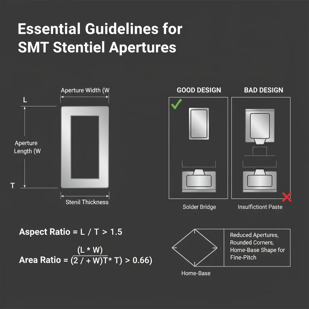
Choosing the Right Solder Paste for Complex Geometries
Not all solder pastes are created equal, especially when dealing with solder paste for complex geometries. The paste must have the right viscosity and composition to flow properly on non-flat surfaces while maintaining stability during the dispensing process. Here are some key factors to consider:
- Particle Size: As mentioned earlier, finer particles (Type 5 or 6) are better suited for small features and textured surfaces common in 3D-MIDs.
- Viscosity: A paste with medium to high viscosity (around 800,000 to 1,200,000 cP) helps prevent slumping on vertical or angled surfaces.
- Flux Type: No-clean fluxes are often preferred for 3D-MIDs, as they reduce the need for post-soldering cleaning, which can be challenging on complex shapes.
Testing different solder pastes under real-world conditions is crucial. For instance, a paste that performs well on flat PCBs might fail to adhere to a curved 3D-MID surface during reflow, leading to defects. Working with a trusted supplier can help identify the best formulation for specific applications.
Overcoming Common Challenges in Solder Paste Application on 3D PCBs
Even with advanced 3D soldering techniques, certain challenges persist when applying solder paste to 3D-MIDs. Let’s explore these, along with solutions to address them.
1. Uneven Paste Distribution
On multi-level or curved surfaces, solder paste can pool in lower areas or fail to reach higher points, leading to inconsistent joints. Using a combination of jet printing and vision-guided robotic systems can help. These tools adjust paste volume based on surface height, ensuring uniform application. For example, a jet printer might deposit 0.1 mg of paste on a lower pad and 0.15 mg on a higher pad to account for gravitational effects during reflow.
2. Accessibility Issues
Some areas of a 3D-MID may be difficult to access due to deep recesses or sharp angles. In such cases, using a tilted or angled dispensing nozzle can improve reach. Additionally, breaking the dispensing process into multiple stages—applying paste to accessible areas first, then adjusting the component orientation for harder-to-reach spots—can enhance coverage.
3. Thermal Stress During Reflow
The varied thickness and material properties of 3D-MIDs can lead to uneven heating during reflow soldering, causing defects like tombstoning or cracking. A tailored reflow profile with gradual temperature ramps (e.g., 1.5°C per second preheat rate) can mitigate this. Advanced ovens with zone-specific temperature control also help ensure uniform heating across the component.
Benefits of Mastering Solder Paste Dispensing on 3D-MIDs
Successfully implementing solder paste dispensing on 3D-MIDs offers several advantages for electronics manufacturers:
- Enhanced Product Reliability: Precise solder paste application reduces defects, leading to more durable and reliable devices. For example, automotive sensors built on 3D-MIDs must withstand harsh conditions, and proper soldering ensures long-term performance.
- Design Flexibility: Mastering 3D soldering techniques allows engineers to push the boundaries of design, creating more compact and innovative products without sacrificing quality.
- Cost Efficiency: Techniques like jet printing minimize material waste and eliminate the need for custom stencils, reducing production costs, especially for small-batch runs.
Future Trends in Solder Paste Application for 3D PCBs
As technology advances, so do the methods for solder paste application on 3D PCBs. One emerging trend is the integration of artificial intelligence (AI) into dispensing systems. AI algorithms can analyze surface geometries in real-time, adjusting dispensing parameters on the fly to optimize paste placement. This is particularly useful for highly variable or custom 3D-MID designs.
Additionally, additive manufacturing techniques are being explored to directly print solder paste alongside conductive traces during the 3D-MID fabrication process. While still in early stages, this approach could streamline production by combining multiple steps into a single workflow, further enhancing precision for solder paste for complex geometries.
Conclusion: Elevating Electronics Manufacturing with 3D-MID Soldering Expertise
Tackling the challenges of solder paste dispensing on 3D-MIDs requires a combination of innovative techniques, specialized equipment, and a deep understanding of material properties. From selective dispensing with jet printing to robotic systems and tailored solder pastes, manufacturers have a range of tools at their disposal to achieve precision on even the most complex geometries. By mastering these 3D soldering techniques, businesses can unlock new possibilities in product design, reliability, and efficiency.
At ALLPCB, we’re committed to supporting engineers and manufacturers in navigating the complexities of modern electronics assembly. Whether you’re working on cutting-edge 3D-MIDs or traditional PCBs, our expertise and resources can help bring your vision to life with unmatched quality. Dive into the world of advanced soldering today and elevate your production capabilities for the future.