 ALLPCB


If you're new to the world of printed circuit boards and wondering, "What is HDI PCB?" or looking for a clear guide on HDI PCB basics, you're in the right place. HDI stands for High-Density Interconnect, a type of PCB designed to pack more components into a smaller space using advanced manufacturing techniques like microvias and fine lines. This technology is essential for modern electronics, from smartphones to medical devices, where size and performance matter. In this beginner's guide, we'll dive deep into HDI PCB basics, explain what makes these boards unique, and provide a step-by-step understanding to help you grasp this cutting-edge technology.
What is HDI PCB? Understanding the Basics
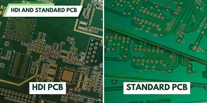
High-Density Interconnect (HDI) PCB is a specialized type of printed circuit board that allows for a higher number of components to be placed in a smaller area. Unlike traditional PCBs, which rely on larger through-holes and wider traces, HDI boards use thinner lines (often less than 75 micrometers) and tiny microvias (holes smaller than 150 micrometers in diameter) to create dense, compact layouts. This results in lighter, smaller, and more efficient electronic devices.
Think of HDI PCBs as the backbone of modern gadgets. They're used in devices where space is limited, but performance can't be compromised—like in smartphones, tablets, and wearable tech. By enabling more connections per square inch, HDI technology supports faster signal transmission and better power efficiency, often achieving signal speeds up to 10 Gbps in high-end applications.
Why HDI PCBs Matter in Modern Electronics
As technology advances, the demand for smaller, faster, and more powerful devices continues to grow. HDI PCBs are at the heart of this evolution for several reasons:
- Miniaturization: HDI boards allow manufacturers to shrink device sizes without sacrificing functionality. For example, a smartphone's motherboard, which once required a much larger PCB, can now fit into a slim design thanks to HDI technology.
- Improved Performance: With shorter trace lengths and reduced signal loss, HDI PCBs support high-speed data transfer. This is critical for applications like 5G devices, where signal integrity is paramount.
- Cost Efficiency in the Long Run: Although HDI PCBs can be more expensive to design and manufacture initially, they reduce the need for multiple boards or larger assemblies, ultimately saving costs in compact designs.
Statistics show that over 49% of electronic devices today rely on HDI technology, a significant shift from traditional designs, as the push for miniaturization continues to dominate the industry.
Key Features of HDI PCBs: What Sets Them Apart
To fully understand HDI PCB basics, let's break down the unique features that distinguish these boards from standard PCBs:
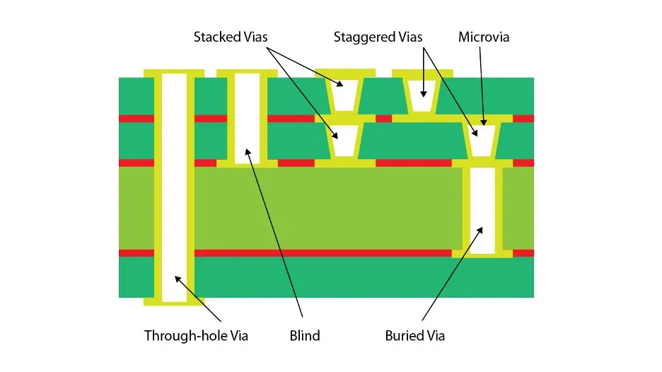
- Microvias: These are tiny holes used to connect different layers of the PCB. Unlike traditional through-holes that go all the way through the board, microvias are laser-drilled and often only connect adjacent layers, saving space. Typical microvia diameters range from 50 to 100 micrometers.
- Fine Lines and Spaces: HDI boards feature trace widths and spaces as small as 50 micrometers, compared to 150 micrometers or more in standard PCBs. This allows for tighter component placement.
- High Layer Count: HDI PCBs often have more layers (sometimes 8 or more) in a thinner profile, enabling complex routing in a compact form.
- Blind and Buried Vias: These vias don't go through the entire board, further optimizing space. Blind vias connect an outer layer to an inner layer, while buried vias connect only internal layers.
How HDI PCBs Are Manufactured: A Simplified Overview
The manufacturing process for HDI PCBs is more complex than for standard boards due to the precision required. Here's a beginner-friendly look at the key steps:
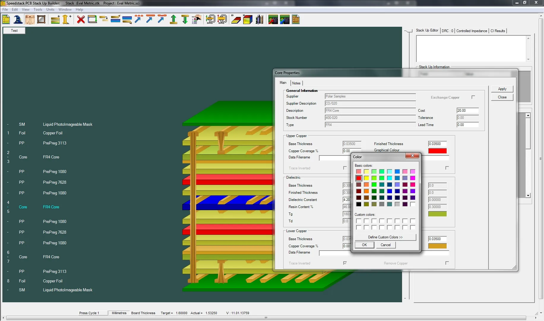
- Design and Planning: Engineers create a detailed layout using specialized software, focusing on via placement and trace routing to maximize density. Stackup planning (arranging layers) is critical to ensure signal integrity.
- Material Selection: High-quality materials like high-Tg (glass transition temperature) laminates are often used to handle the thermal stress of compact designs. Common materials include FR-4 with enhanced properties or polyimide for flexibility.
- Laser Drilling: Microvias are created using laser drilling, which offers precision for holes as small as 50 micrometers. This step replaces mechanical drilling used in traditional PCBs.
- Layer Bonding: Multiple layers are stacked and bonded under heat and pressure. This process must be precise to avoid misalignment of microvias.
- Plating and Etching: Copper is plated into the microvias to establish connections, and excess material is etched away to form fine traces.
- Testing: Rigorous testing ensures that the board meets impedance requirements (often targeting values like 50 ohms for high-speed signals) and has no defects.
This process requires advanced equipment and expertise, which is why partnering with a reliable PCB manufacturer is crucial for quality results.
Applications of HDI PCBs: Where Are They Used?
HDI PCBs are a game-changer in industries where compact, high-performance electronics are essential. Here are some common applications:
- Consumer Electronics: Smartphones, tablets, and laptops rely on HDI boards to fit complex circuits into sleek designs. For instance, modern phone motherboards often use 6-8 layer HDI PCBs.
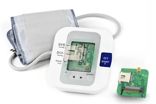
- Medical Devices: Wearable health monitors and implantable devices use HDI technology for their small size and reliability.
- Automotive Systems: Advanced driver-assistance systems (ADAS) and infotainment systems use HDI PCBs to handle high-speed data and ensure durability.
- Aerospace and Defense: HDI boards are used in compact, high-reliability systems like satellites and avionics, where weight and space are critical factors.
Benefits and Challenges of HDI PCBs for Beginners
Understanding the pros and cons of HDI PCBs can help you decide if they're the right choice for your project. Let's explore both sides:
Benefits of HDI PCBs
- Space Efficiency: More components in less space means smaller, lighter products.
- Better Signal Integrity: Shorter traces reduce noise and improve performance, especially for high-frequency signals above 1 GHz.
- Flexibility in Design: HDI allows for creative layouts, supporting innovative product designs.
Challenges of HDI PCBs
- Higher Cost: The advanced materials and precision manufacturing increase production costs compared to standard PCBs.
- Design Complexity: Creating an HDI layout requires expertise in stackup design, via placement, and thermal management.
- Manufacturing Limitations: Not all manufacturers have the technology or experience to produce high-quality HDI boards, so choosing the right partner is essential.
Tips for Getting Started with HDI PCB Design
If you're new to HDI PCB design, here are some practical tips to help you navigate the process:
- Learn the Basics of PCB Design First: Before diving into HDI, familiarize yourself with standard PCB design principles like layer stacking and trace routing.
- Use the Right Tools: Invest in design software that supports HDI features, such as microvia placement and fine-line routing.
- Focus on Stackup Planning: A well-planned layer arrangement is critical to avoid signal interference and ensure manufacturability.
- Partner with Experts: Work with a trusted manufacturer who understands HDI technology and can guide you through material selection and testing.
- Start Small: Begin with simpler HDI designs (e.g., 1+N+1 structure, meaning one build-up layer on each side of the core) before moving to complex multi-layer boards.
Future Trends in HDI PCB Technology
As electronics continue to evolve, HDI PCB technology is also advancing. Here are a few trends to watch:
- Smaller Microvias: Advances in laser drilling are pushing microvia sizes below 50 micrometers, allowing even denser designs.
- Integration with Flexible PCBs: Combining HDI with flexible materials is opening new possibilities for foldable and wearable devices.
- Enhanced Thermal Management: New materials and designs are being developed to handle the heat generated by high-density circuits, critical for applications like 5G and AI hardware.
Conclusion: Why HDI PCBs Are the Future of Electronics
High-Density Interconnect (HDI) PCBs are revolutionizing the way we design and build electronics. By allowing more components to fit into smaller spaces with improved performance, they’re enabling the next generation of compact, high-speed devices. Whether you're an engineer just starting out or a hobbyist curious about advanced PCB technology, understanding HDI PCB basics is a valuable step toward mastering modern electronics.
This HDI PCB guide for beginners has covered the essentials—from what HDI PCBs are and how they’re made to their applications and design challenges. With this foundation, you’re better equipped to explore the world of high-density interconnect technology and apply it to your projects. Remember, partnering with a reliable PCB manufacturer can make all the difference in turning your HDI designs into reality.


