ALLPCB


Budget-Friendly Builds: Cost Optimization Strategies for Gaming PCBs
Gaming systems demand printed circuit boards that handle high data rates, dense component placement, and sustained thermal loads. Engineers and procurement teams often seek ways to manage expenses while preserving signal integrity and reliability. Cost optimization for gaming PCBs focuses on material selection, layout efficiency, and assembly processes that align with performance requirements. These approaches help teams deliver capable hardware within defined budgets without introducing unnecessary complexity.
Why Cost Optimization Matters in Gaming PCB Projects
Gaming applications push boards toward multilayer constructions, controlled impedance traces, and robust power distribution networks. Each additional layer or specialized process raises manufacturing expenses and extends lead times. Effective PCB manufacturing cost reduction strategies allow teams to maintain functionality while trimming avoidable expenditures. Procurement specialists benefit when designs incorporate standard panel sizes and common material grades from the outset. This alignment reduces waste and simplifies sourcing across production runs.
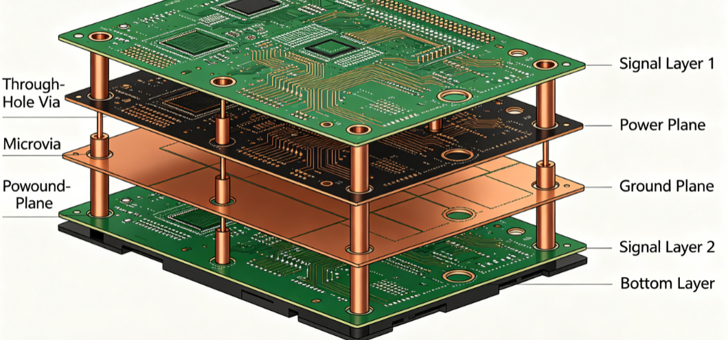
Technical Principles Behind Cost Drivers
Material choices directly influence both performance and expense. Standard FR-4 laminates provide adequate electrical and mechanical properties for many gaming boards when operating frequencies remain within typical ranges. Alternative PCB materials, such as modified epoxy systems with lower resin content, can lower overall board weight and material usage while supporting required thermal performance. Layer count and via structures also affect pricing; reducing the number of sequential lamination steps through careful stack-up planning limits processing time.
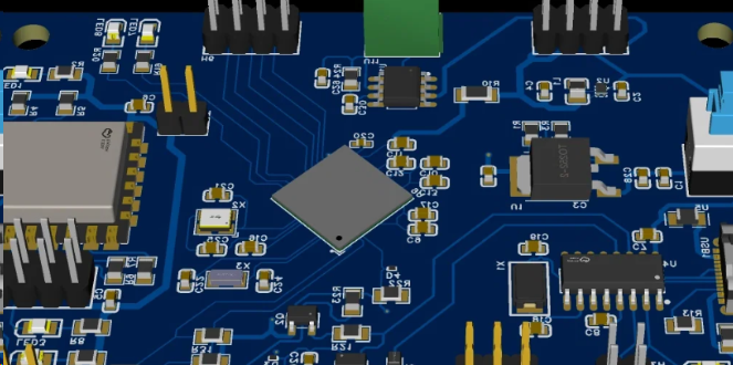
Signal integrity requirements in gaming layouts often necessitate controlled impedance routing and ground planes. Efficient PCB layout techniques minimize the total copper area and via count by grouping high-speed signals logically and optimizing return paths. Thermal management considerations, including copper pours and thermal vias, must balance heat dissipation against added fabrication steps. These engineering decisions follow established qualification practices that verify board performance under expected conditions.
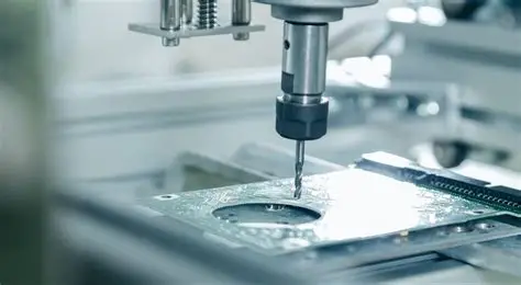
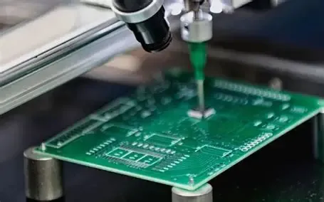
Practical Solutions for Affordable PCB Assembly and Production
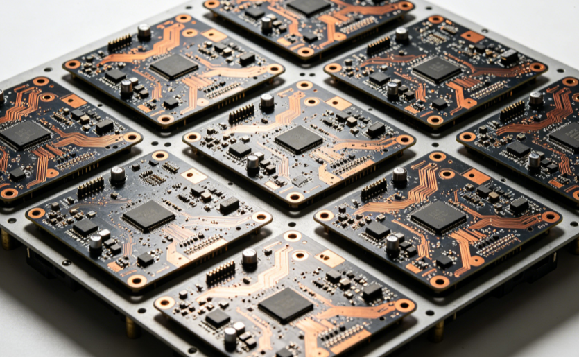
Design for manufacturability practices form the foundation of affordable PCB assembly. Early collaboration between layout engineers and fabrication teams identifies opportunities to standardize hole sizes, trace widths, and spacing rules that match common production capabilities. Panelization strategies that maximize board count per panel reduce per-unit processing costs while maintaining handling integrity during assembly.
Component placement optimization further supports cost control. Grouping similar parts and aligning orientations simplifies automated placement and inspection routines. Selective use of surface-mount technology for most components, combined with through-hole only where mechanically necessary, streamlines the assembly sequence. Solder mask and silkscreen choices also influence expense; standard colors and thicknesses avoid premium processing fees while meeting functional needs.
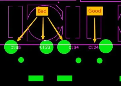
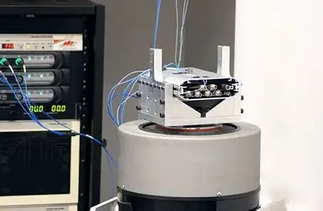
Quality verification remains essential throughout these optimizations. Boards undergo electrical testing and visual inspection to confirm conformance with performance specifications. Industry standards guide these checks to ensure consistent results across batches.
Layout Efficiency and Material Alternatives in Practice
Engineers apply efficient PCB layout techniques by reviewing trace routing density and via placement early in the design cycle. Shorter signal paths and fewer layer transitions reduce both material usage and potential signal degradation points. When high-frequency performance allows, substituting certain high-speed layers with standard dielectric materials cuts expenses without measurable impact on gameplay responsiveness.
Alternative PCB materials enter consideration when thermal or mechanical demands permit. Lower-cost laminates with appropriate glass transition temperatures and dielectric constants support many gaming requirements when paired with proper copper weight selection. These substitutions undergo evaluation against mechanical stress and environmental exposure criteria to confirm suitability.
Maintaining Quality During Cost Reduction
Cost optimization never overrides reliability targets. Teams reference established qualification specifications to validate that reduced-layer or alternative-material designs still meet mechanical, electrical, and environmental requirements. Visual and automated optical inspection steps catch deviations before assembly proceeds. This disciplined approach prevents downstream failures that could erase initial savings.
Conclusion
Cost optimization for gaming PCBs succeeds when material, layout, and assembly decisions integrate from the initial concept stage. Alternative PCB materials and efficient PCB layout techniques deliver meaningful reductions when applied within performance boundaries. Affordable PCB assembly follows from standardized processes and early manufacturability reviews. These methods support competitive builds while upholding the reliability expected in gaming hardware.
FAQs
Q1: How does cost optimization for gaming PCBs balance performance and expense?
A1: Engineers evaluate material grades, layer counts, and routing density against required signal speeds and thermal loads. Standard laminates and simplified stack-ups often suffice when designs incorporate efficient PCB layout techniques from the start. This measured approach achieves PCB manufacturing cost reduction while preserving gameplay-critical functions.
Q2: What role do alternative PCB materials play in PCB manufacturing cost reduction?
A2: Alternative PCB materials with adjusted resin systems or glass styles can lower raw material expenses when electrical and thermal specifications permit their use. Selection follows verification against mechanical and environmental criteria to ensure long-term stability in gaming environments.
Q3: Which efficient PCB layout techniques most effectively support affordable PCB assembly?
A3: Techniques such as minimizing via counts, standardizing hole sizes, and optimizing component orientation reduce both fabrication steps and assembly time. These practices align with common production capabilities and decrease the likelihood of rework during soldering and inspection.
Q4: How can teams ensure quality while pursuing cost optimization for gaming PCBs?
A4: Quality remains anchored through adherence to defined inspection and testing protocols at each stage. Electrical continuity checks and visual verification confirm that optimizations do not compromise board integrity before final integration into gaming systems.
References
IPC-6012E — Qualification and Performance Specification for Rigid Printed Boards. IPC, 2017
IPC-A-600K — Acceptability of Printed Boards. IPC, 2020