 ALLPCB


What Is PTH and Why It Matters
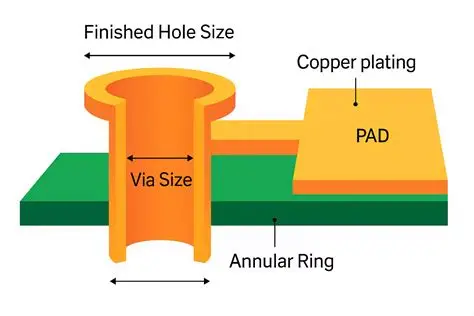
A plated through-hole consists of a drilled opening in the PCB that receives a conductive metal coating, typically copper, along its walls. This plating forms a continuous electrical path between different layers of the board. PTH differs from surface-mount methods by offering stronger physical anchoring for larger components such as connectors, switches, and power devices. For hobbyists, PTH design supports straightforward hand soldering and rework, which reduces the learning curve when building prototypes or one-off projects.
The relevance of PTH extends to mixed-technology boards that combine through-hole and surface-mount parts. Hobbyists often choose PTH when projects require frequent component changes or when boards experience mechanical stress. Proper PTH implementation improves overall board reliability by distributing forces away from solder joints. Industry standards guide these practices to ensure consistent performance across designs.
Technical Principles of PTH Formation
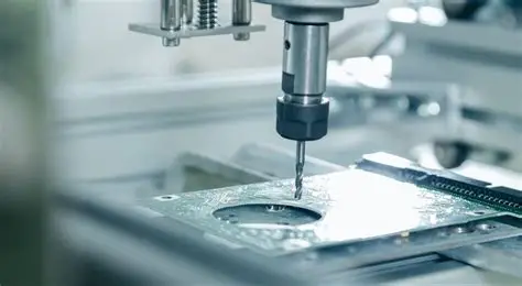
The process begins with drilling precise holes through the substrate material. After drilling, a thin seed layer of copper is deposited on the hole walls through electroless plating. Subsequent electrolytic plating builds up the copper thickness to meet electrical and mechanical requirements. This layered structure creates a robust via that carries current while maintaining structural integrity.
Key factors include hole diameter, plating thickness, and aspect ratio, which is the relationship between board thickness and hole diameter. High aspect ratios demand careful control to avoid voids or incomplete plating. Thermal expansion differences between the copper and substrate can induce stress during temperature cycling, so designers account for these effects in material selection. IPC-6012E outlines qualification requirements for rigid printed boards, including criteria for plating integrity and hole quality.
PTH Design Steps for Hobbyists
Effective PTH design follows a logical sequence that begins with schematic capture and component placement. After defining the circuit, the designer selects hole sizes based on component lead diameters and current-carrying needs. Software tools for PTH design allow users to set drill sizes, pad diameters, and clearance rules that comply with manufacturing capabilities.
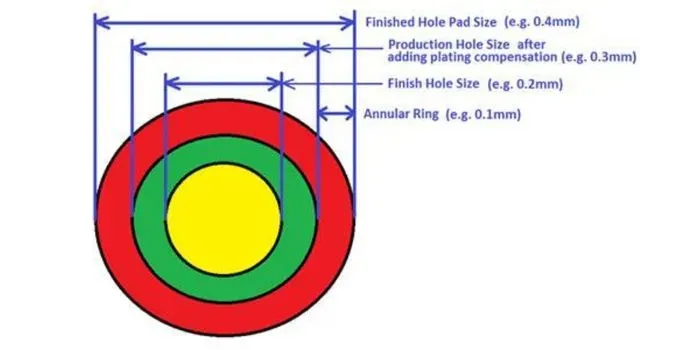
Next, the layout incorporates appropriate annular rings around each hole to provide soldering area and tolerance for misalignment. Routing traces away from dense hole clusters prevents crowding and supports clean etching. Simulation features in PTH design software help verify signal integrity and thermal performance before fabrication. These PTH design steps ensure the board meets both functional and producibility goals.
Best Practices in PTH Layout and Verification
Designers maintain minimum distances between holes and board edges to avoid structural weakness. Pad sizes typically exceed the finished hole diameter by a sufficient margin to accommodate plating and soldering variations. When mixing PTH with other technologies, separate zones on the board reduce interference during assembly.
Verification includes checking for adequate copper thickness in the holes and confirming that no unintended connections exist. Visual inspection of prototypes reveals issues such as incomplete plating or drill wander. Following these practices aligns with IPC-A-600K guidance on acceptability of printed boards, which defines criteria for hole wall quality and surface features.
Conclusion
PTH design basics provide hobbyists with a reliable method for creating durable and serviceable circuit boards. By following structured PTH design steps and using appropriate PTH design software features, builders achieve consistent results across projects. Attention to plating quality, hole sizing, and layout clearances supports long-term performance. These fundamentals help newcomers progress from simple prototypes to more complex assemblies while meeting recognized industry expectations.
FAQs
Q1: What are the essential PTH design basics every hobbyist should know?
A1: PTH design basics cover hole sizing, pad dimensions, plating thickness, and clearance rules that ensure reliable electrical and mechanical connections. Hobbyists benefit from starting with standard hole diameters that match common component leads and verifying aspect ratios to avoid plating defects. These elements form the foundation for boards that withstand repeated assembly and use.
Q2: How to design PTH layouts effectively in software?
A2: Learning how to design PTH involves setting drill files, defining annular rings, and applying design rules that match fabrication limits within PTH design software. Users place components first, then route traces while maintaining adequate spacing around holes. Simulation tools within the software help identify potential thermal or signal issues early in the process.
Q3: What PTH design steps improve success for beginners?
A3: PTH design steps typically include schematic review, component footprint selection, hole and pad definition, trace routing, and design rule checks. Hobbyists should also generate manufacturing outputs such as drill files and verify them against board thickness. Following this sequence reduces errors and produces boards ready for straightforward assembly.
Q4: Which standards guide PTH quality for hobbyist projects?
A4: Standards such as IPC-6012E and IPC-A-600K provide acceptance criteria for plating thickness, hole wall condition, and overall board quality. Hobbyists who reference these documents during design and inspection achieve more consistent outcomes. Applying the guidelines helps ensure boards meet basic reliability expectations without requiring specialized equipment.
IPC-6012E: Qualification and Performance Specification for Rigid Printed Boards
IPC-A-600K: Acceptability of Printed Boards





