ALLPCB


Introduction
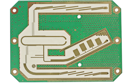
In printed circuit board design, the top layer serves multiple functions beyond signal routing and component placement. Silkscreen, also known as the legend layer, provides essential markings for assembly and identification. When thermal management becomes a priority, designers must evaluate how silkscreen interacts with heat flow paths on the top layer. Poor placement can impede heat dissipation from components or copper planes. Effective integration of silkscreen considerations supports reliable operation in high-power or dense layouts. This approach aligns with established engineering practices for balancing functionality and thermal performance.
What Is Silkscreen and Why Thermal Management Matters
Silkscreen consists of non-conductive ink applied to the outer layers of a PCB to mark component outlines, reference designators, polarity indicators, and other assembly information. The ink typically exhibits low thermal conductivity compared with copper traces or planes. In applications involving heat sensitive components, such as power semiconductors or processors, unmanaged heat buildup can lead to performance degradation or reduced lifespan. PCB thermal management addresses these issues through material selection, layout techniques, and layer stackup decisions. Silkscreen placement directly influences whether heat radiates effectively from exposed copper areas or becomes partially insulated. Considering these factors early in the design process helps maintain consistent operating temperatures across the board.
Technical Principles of Silkscreen and Heat Dissipation
Silkscreen ink forms a thin layer that covers portions of the top copper without contributing to electrical conduction or significant heat spreading. Its thermal properties limit radiative and convective cooling when applied over large copper areas intended for heat sinking. In contrast, exposed copper surfaces allow better heat transfer to the surrounding environment or attached heatsinks. Thermal vias, which are plated holes connecting layers, provide vertical heat paths that bypass surface obstructions. When silkscreen overlaps via pads or thermal relief patterns, it can reduce the effective surface area available for heat transfer. Component placement relative to these features further determines local temperature gradients. Understanding these interactions supports layout decisions that prioritize both readability and thermal efficiency.
Practical Solutions and Best Practices for Top Layer Design
Designers begin by identifying high-heat zones during component placement and routing. Silkscreen should avoid covering thermal pads, large copper pours, or areas directly beneath heat generating devices. Instead, markings can be positioned on adjacent non-critical regions or moved to the bottom layer where feasible. Thermal vias placed under components benefit from clearance in the silkscreen layer to preserve maximum contact area for heatsink attachment or airflow. Standard design rules recommend maintaining minimum distances between silkscreen elements and heat-sensitive features to prevent unintended insulation effects. Review of the top layer artwork includes checking for silkscreen overlap on via arrays or exposed copper intended for cooling. These steps integrate with overall PCB thermal management strategies without compromising assembly instructions.
Additional practices involve using thinner silkscreen ink where coverage is unavoidable or selecting ink formulations with improved thermal characteristics when available. Simulation tools can model temperature distributions with and without silkscreen coverage to validate layout choices. In multilayer boards, internal copper planes often carry the primary heat load, reducing reliance on top-layer radiation. Coordination between the silkscreen layer and solder mask ensures that mask-defined openings align with thermal requirements. Regular design reviews help catch placement conflicts before fabrication.
Best Practices for Heat Sensitive Components
Heat sensitive components require dedicated cooling strategies that extend to silkscreen decisions. Placement of these parts near board edges or in areas with good airflow improves baseline thermal performance. Silkscreen around such components should remain minimal and positioned to avoid blocking any intended heat spreader contact. Thermal vias connected to internal planes or bottom-side copper further enhance dissipation when silkscreen clearance is maintained. Documentation of these considerations in the design files supports consistent manufacturing outcomes. Following these guidelines reduces the risk of localized overheating during operation.
Conclusion
Silkscreen and thermal management intersect at the top layer through careful planning of ink placement, via usage, and copper exposure. Logical evaluation of heat paths alongside marking requirements leads to balanced designs. Application of these principles supports reliable performance for heat sensitive components and overall board integrity. Early attention to silkscreen thermal properties during layout minimizes later revisions.
FAQs
Q1: How does silkscreen affect PCB thermal management?
A1: Silkscreen ink covers portions of the top layer and exhibits low thermal conductivity, which can reduce heat dissipation from exposed copper areas. Proper placement avoids critical thermal paths while preserving necessary markings for assembly. This consideration integrates with techniques such as thermal vias to maintain effective cooling.
Q2: What are the thermal properties of silkscreen ink in PCB design?
A2: Silkscreen ink generally provides electrical insulation and identification but offers minimal contribution to heat spreading due to its composition. Designers account for this by limiting coverage over copper planes or thermal features. The result supports better overall heat transfer when combined with appropriate layout practices.
Q3: Why consider silkscreen placement for cooling around heat sensitive components?
A3: Heat sensitive components benefit from unobstructed copper surfaces and thermal vias for heat removal. Silkscreen positioned over these areas may partially insulate the surface and affect local temperatures. Strategic relocation of markings helps preserve cooling efficiency without sacrificing identification needs.
Q4: How do thermal vias interact with silkscreen on the top layer?
A4: Thermal vias transfer heat vertically through the board and often require exposed pads for optimal performance. Silkscreen should maintain clearance around via arrays to avoid reducing the effective heat transfer area. This approach enhances the contribution of vias to PCB thermal management strategies.
References
IPC-6012E - Qualification and Performance Specification for Rigid Printed Boards. IPC, 2017
IPC-A-600K - Acceptability of Printed Boards. IPC, 2020
JEDEC J-STD-020E - Moisture/Reflow Sensitivity Classification. JEDEC, 2014