 ALLPCB


Introduction
Automotive electronics demand printed circuit boards that maintain performance under extreme conditions. Blind and buried vias enable higher component density while supporting the reliability needed in vehicles. These via types help designers meet requirements for vibration resistance and thermal stability in automotive PCB applications. Engineers select them to improve signal integrity and reduce board size without compromising via reliability. The approach aligns with established industry practices for multilayer constructions used in engine control units, sensors, and infotainment systems.
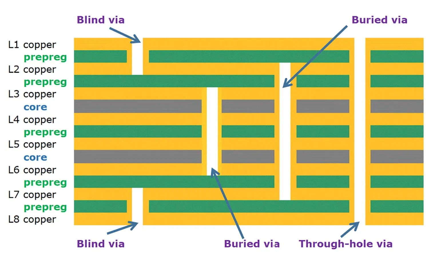
Understanding Blind and Buried Vias
Blind vias connect an outer layer to one or more inner layers without extending through the entire board thickness. Buried vias link only internal layers and remain invisible from the outer surfaces. Both types differ from conventional through-hole vias by limiting the drilled path, which reduces parasitic effects and supports finer routing. In automotive PCB designs, these features allow more compact layouts while preserving the mechanical integrity required for high-temperature PCB environments. Designers evaluate stack-up configurations early to determine where blind or buried vias provide the greatest benefit for signal paths and power distribution.
Why These Vias Matter in Automotive Electronics
Automotive environments expose PCBs to continuous vibration, rapid temperature changes, and long operational lifetimes. Via reliability becomes a primary concern because any fracture or delamination can lead to intermittent failures in safety-critical systems. Blind and buried vias contribute to vibration resistance by shortening the copper barrel length and reducing stress concentration points compared with full through vias. They also support the dense interconnects needed for modern automotive electronics without increasing overall board thickness. Meeting these demands requires careful attention to material selection and manufacturing processes that maintain structural stability across the full temperature range.
Technical Principles and Reliability Factors
The mechanical behavior of vias under thermal cycling depends on copper thickness, plating quality, and the coefficient of thermal expansion mismatch between copper and dielectric materials. Shorter via barrels in blind and buried constructions experience lower cumulative stress during repeated expansion and contraction. This characteristic improves long-term via reliability in high-temperature PCB applications. Electrical performance also benefits because reduced via length lowers inductance and improves return paths for high-speed signals common in automotive electronics. Manufacturing must control drill aspect ratios and plating uniformity to avoid voids or thin spots that could initiate cracks under vibration.
Design rules typically specify minimum annular ring sizes and copper weights that maintain adequate current-carrying capacity while fitting within the constrained space of blind or buried features. Thermal management considerations include the placement of these vias near heat-generating components to aid heat spreading without creating weak points. Engineers analyze finite element models of the board under simulated vibration profiles to verify that the chosen via configuration will endure expected service conditions. These analyses incorporate the effects of different laminate materials and their behavior at elevated temperatures.
Practical Design and Manufacturing Considerations
Effective implementation begins with defining clear via type requirements during the schematic and layout phases. Designers document stack-up details and via start-stop layers so fabricators can apply appropriate sequential lamination or laser drilling processes. Aspect ratio limits for blind vias are generally tighter than for through vias to ensure reliable plating. Material choices focus on laminates with stable glass transition temperatures and low moisture absorption to support high-temperature PCB performance.
Collaboration between design and manufacturing teams helps identify potential issues such as registration tolerances between layers or drill wander that could affect via integrity. Inspection protocols emphasize cross-sectional analysis at critical via locations to confirm plating thickness and fill quality. These steps align with qualification approaches outlined in IPC-6012E for rigid printed boards.
Best Practices for Ensuring Via Reliability
Engineers apply conservative design margins for annular ring and copper thickness when specifying blind or buried vias in automotive applications. They also consider the cumulative effect of multiple thermal excursions during assembly and field operation. Vibration resistance improves when via locations avoid high-flexure zones and when additional copper reinforcement is added where feasible. Process controls during plating and lamination reduce the incidence of defects that could compromise long-term performance.
Testing programs typically include thermal shock, temperature cycling, and mechanical vibration sequences that replicate automotive duty cycles. Results guide iterative refinements to via dimensions or material selections. Documentation of these activities supports traceability and helps maintain consistency across production lots.
Conclusion
Blind and buried vias offer practical advantages for achieving the density and reliability targets of modern automotive PCB designs. Their shorter barrel lengths reduce stress under thermal and mechanical loads, supporting the vibration resistance and via reliability demanded by automotive electronics. Structured design reviews, adherence to material and process controls, and verification testing provide the foundation for consistent performance. When implemented according to established engineering practices, these via types help meet the stringent requirements of high-temperature PCB environments without unnecessary complexity.
FAQs
Q1: How do blind and buried vias improve via reliability in automotive PCB designs?
A1: Blind and buried vias shorten the copper barrel length compared with through-hole vias, which reduces mechanical stress during thermal cycling and vibration. This configuration helps maintain electrical continuity in automotive electronics exposed to temperature extremes and mechanical shock. Proper plating thickness and material selection further enhance long-term performance under these conditions.
Q2: What role do industry standards play in specifying blind and buried vias for high-temperature PCB applications?
A2: Standards such as IPC-6012E establish qualification requirements for rigid printed boards, including criteria for via construction and plating integrity. These guidelines help ensure that automotive PCBs meet performance expectations across temperature ranges and vibration profiles. Manufacturers reference the same documents during process control and acceptance testing.
Q3: Why is vibration resistance a key consideration when using blind and buried vias in automotive electronics?
A3: Vibration can induce fatigue in via barrels and surrounding copper features over time. Shorter via paths in blind and buried constructions experience lower stress amplitudes, improving resistance to crack initiation. Design practices that locate vias away from high-flexure areas and maintain adequate annular rings further support durability in vehicle environments.
Q4: How does stack-up planning affect the successful use of blind and buried vias in automotive PCB layouts?
A4: Stack-up planning determines the exact layers connected by each via type and influences drill depth, aspect ratio, and registration accuracy. Careful definition of these parameters supports reliable plating and minimizes defects that could affect via reliability. Early coordination with fabrication requirements helps achieve the density and performance targets typical of automotive electronics.


