 ALLPCB


If you're looking to understand the ins and outs of FR-4 PCB manufacturing, you've come to the right place. This guide dives deep into the FR-4 PCB manufacturing process flow, offers a detailed FR-4 PCB material selection guide, and shares best practices for FR-4 PCB design, FR-4 PCB layer stackup optimization, and FR-4 PCB thermal management techniques. Whether you're an engineer, designer, or hobbyist, this comprehensive resource will equip you with actionable insights to create high-quality printed circuit boards.
Let’s explore everything from raw materials to final assembly, ensuring you have the knowledge to optimize performance and reliability in your projects.
What is FR-4 and Why is it So Popular in PCB Manufacturing?
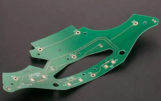
FR-4, short for Flame Retardant 4, is a widely used material for printed circuit boards (PCBs). It is a composite made of woven fiberglass cloth and epoxy resin, offering a balance of durability, affordability, and electrical insulation. This material is the go-to choice for many applications, from consumer electronics to industrial equipment, due to its excellent mechanical strength and resistance to heat and moisture.
Its popularity stems from its versatility. FR-4 can handle a wide range of operating temperatures (typically up to 130°C) and provides a dielectric constant of around 4.5, making it suitable for most standard electronic designs. Understanding FR-4 is the foundation of mastering PCB manufacturing, and this guide will break down every aspect of working with it.
FR-4 PCB Manufacturing Process Flow: Step by Step
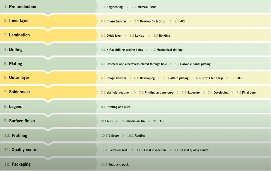
The journey of creating an FR-4 PCB involves several precise steps. Below is a detailed look at the FR-4 PCB manufacturing process flow to give you a clear picture of how raw materials transform into functional circuit boards.
1. Material Preparation
The process begins with preparing the FR-4 substrate. Sheets of woven fiberglass are impregnated with epoxy resin and partially cured to form prepreg layers. These layers are then cut to size based on the PCB design specifications.
2. Inner Layer Processing
For multilayer boards, the inner copper layers are etched with the circuit pattern. This involves laminating a thin copper foil onto the FR-4 substrate, applying a photoresist layer, exposing it to UV light through a mask, and etching away unwanted copper with chemicals.
3. Lamination
Multiple layers of prepreg and copper-clad FR-4 are stacked and pressed together under high heat (around 170-180°C) and pressure. This bonds the layers into a single, solid panel.
4. Drilling
Holes for vias and component mounting are drilled into the board using high-precision CNC machines. These holes often have a diameter as small as 0.2 mm, depending on the design requirements.
5. Plating and Outer Layer Processing
The drilled holes are plated with copper to create electrical connections between layers. The outer layers are then etched with the final circuit pattern, similar to the inner layer process.
6. Solder Mask and Silkscreen Application
A protective solder mask (usually green) is applied to prevent short circuits and oxidation. A silkscreen layer is added for labeling components and other markings, typically in white ink.
7. Surface Finish
A surface finish, such as HASL (Hot Air Solder Leveling) or ENIG (Electroless Nickel Immersion Gold), is applied to the exposed copper to enhance solderability and protect against corrosion.
8. Testing and Cutting
The finished board undergoes electrical testing to check for continuity and shorts. Finally, the panel is cut into individual PCBs using routing or V-scoring techniques.
FR-4 PCB Material Selection Guide: Choosing the Right Variant
Not all FR-4 materials are created equal. The FR-4 PCB material selection guide below will help you pick the right type based on your project needs, ensuring optimal performance and cost-efficiency.
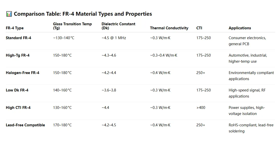
Standard FR-4
This is the most common type, suitable for general-purpose applications. It has a glass transition temperature (Tg) of around 130°C and a dielectric constant of 4.5-4.7. Use this for low-frequency circuits and basic consumer electronics.
High-Tg FR-4
For designs exposed to higher temperatures, high-Tg FR-4 (Tg of 150-180°C) is ideal. It offers better thermal stability and is often used in automotive and industrial applications where heat resistance is critical.
Low-Dk FR-4
If your project involves high-frequency signals (above 1 GHz), consider low-Dk (dielectric constant) FR-4 variants. These materials reduce signal loss and are suitable for RF and microwave applications.
Halogen-Free FR-4
For environmentally conscious designs, halogen-free FR-4 is a great choice. It avoids harmful chemicals while maintaining flame-retardant properties, aligning with RoHS compliance standards.
When selecting a material, consider factors like operating temperature, frequency requirements, and budget. Always consult with your manufacturing partner to ensure compatibility with their processes.
Best Practices for FR-4 PCB Design
Designing an FR-4 PCB requires careful planning to avoid performance issues. Follow these best practices for FR-4 PCB design to ensure functionality and reliability.
1. Maintain Proper Trace Width and Spacing
For standard 1 oz copper thickness, a minimum trace width of 6 mils (0.15 mm) and spacing of 6 mils is recommended for most designs. Adjust these based on current-carrying requirements using online calculators or IPC-2221 standards.
2. Minimize Signal Crosstalk
Keep high-speed signal traces away from each other or use ground planes to shield them. Maintain at least 3x the trace width as spacing for signals operating above 100 MHz to reduce interference.
3. Use Proper Via Sizes
Opt for via diameters of 10-12 mils for standard designs to ensure reliable connections without compromising board strength. Smaller vias (below 8 mils) may increase manufacturing costs.
4. Plan for Component Placement
Place components logically, grouping related parts together to minimize trace lengths. Keep heat-generating components away from sensitive areas to avoid thermal stress on the FR-4 material.
5. Follow Design for Manufacturability (DFM) Guidelines
Ensure your design aligns with manufacturing capabilities, such as minimum hole sizes and tolerances. This reduces errors and lowers production costs.
FR-4 PCB Layer Stackup Optimization: Building for Performance
The arrangement of layers in a multilayer PCB, or stackup, plays a critical role in signal integrity and EMI control. Here’s how to approach FR-4 PCB layer stackup optimization for the best results.
Common Stackup for 4-Layer Boards
A typical 4-layer FR-4 PCB stackup includes:
- Top Layer: Signal traces and components
- Inner Layer 1: Ground plane
- Inner Layer 2: Power plane
- Bottom Layer: Signal traces
This setup provides good EMI shielding and power distribution. The ground plane should be kept as continuous as possible to minimize impedance mismatches.
Stackup for 8-Layer Boards
For more complex designs, an 8-layer stackup might look like this:
- Top: Signal
- Layer 2: Ground
- Layer 3: Signal
- Layer 4: Power
- Layer 5: Power
- Layer 6: Signal
- Layer 7: Ground
- Bottom: Signal
This configuration balances signal layers with dedicated power and ground planes, reducing noise in high-speed designs.
Tips for Optimization
Ensure symmetry in the stackup to prevent warping during manufacturing. Keep high-speed signals on layers adjacent to ground planes to control impedance (typically targeting 50 ohms for single-ended traces). Lastly, use FR-4 prepreg thicknesses (e.g., 0.1-0.2 mm) that match your dielectric constant needs for consistent performance.
FR-4 PCB Thermal Management Techniques: Keeping Cool Under Pressure
Heat can degrade FR-4 PCB performance, so effective thermal management is essential. These FR-4 PCB thermal management techniques will help maintain reliability in demanding applications.
1. Use Thermal Vias
Place thermal vias under heat-generating components like power ICs to transfer heat to a ground plane or heat sink. A grid of 0.3 mm vias spaced 1.2 mm apart can reduce temperatures by up to 10-15°C in high-power areas.
2. Incorporate Copper Pours
Add large copper pours connected to ground or power planes near hot components. This increases the thermal mass and helps dissipate heat across the board.
3. Optimize Component Placement
Distribute heat sources evenly across the PCB to avoid hotspots. Place sensitive components away from high-heat areas to prevent performance degradation.
4. Consider Thicker Copper Layers
For high-current applications, use 2 oz or 3 oz copper instead of the standard 1 oz. Thicker copper improves heat dissipation but may increase costs.
5. Add External Cooling
In extreme cases, attach heat sinks or fans to the PCB. Ensure mounting holes or thermal pads are designed into the board for secure attachment.
FR-4 has a thermal conductivity of about 0.3 W/m·K, which is low compared to metal-core boards. If your application exceeds FR-4’s limits (above 130°C for standard variants), consider upgrading to high-Tg materials or alternative substrates.
Common Challenges in FR-4 PCB Manufacturing and How to Avoid Them
Even with careful planning, issues can arise during FR-4 PCB production. Here are some common challenges and solutions to keep your project on track.
Delamination
Delamination occurs when layers separate due to poor bonding or thermal stress. To prevent this, ensure proper lamination conditions (temperature and pressure) and avoid excessive heat cycles during assembly.
Signal Integrity Issues
Poor stackup design or inadequate grounding can cause signal loss or crosstalk. Use controlled impedance traces and follow stackup guidelines to maintain signal quality.
Warping
Uneven copper distribution or asymmetrical stackups can lead to board warping. Balance copper across layers and maintain symmetry in multilayer designs.
Conclusion: Mastering FR-4 PCB Manufacturing
FR-4 remains the backbone of PCB manufacturing due to its affordability, reliability, and versatility. By understanding the FR-4 PCB manufacturing process flow, following the FR-4 PCB material selection guide, adhering to best practices for FR-4 PCB design, optimizing FR-4 PCB layer stackup, and applying effective FR-4 PCB thermal management techniques, you can create high-performing circuit boards tailored to your needs.
Whether you're designing a simple prototype or a complex multilayer board, the tips and insights in this guide will help you achieve success. Partner with a trusted manufacturing service to bring your FR-4 PCB designs to life with precision and quality.


