 ALLPCB


When deciding between sequential build-up PCB manufacturing and traditional PCB manufacturing, the right choice depends on your project's specific needs, budget, and performance goals. Sequential build-up (SBU) offers advantages for high-density, complex designs with better signal integrity, but it often comes at a higher cost. Traditional PCB manufacturing, on the other hand, is more cost-effective and suitable for simpler, less demanding applications. In this comprehensive guide, we’ll dive into a detailed comparison, including a sequential build-up PCB cost analysis, the pros and cons of sequential build-up PCB vs standard PCB, and insights on when to use sequential build-up PCB. Let’s explore which method aligns best with your project.
What Are Sequential Build-Up and Traditional PCB Manufacturing?
Before we compare the two methods, let’s clarify what each entails. Understanding the basics will help you grasp their differences and applications.
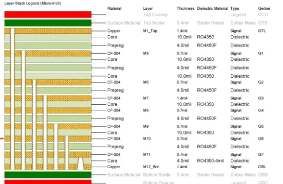
Traditional PCB Manufacturing refers to the standard process of creating printed circuit boards (PCBs) using a laminated structure of conductive copper layers and insulating substrates. Layers are stacked and bonded together in a single pressing operation, with vias (holes) drilled to connect layers. This method has been the backbone of electronics for decades and works well for many applications.
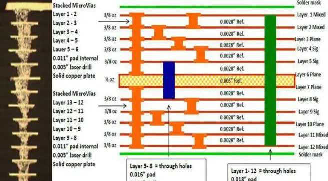
Sequential Build-Up (SBU) PCB Manufacturing, also known as high-density interconnect (HDI) technology, builds the PCB layer by layer. Each layer is added sequentially, with microvias (tiny holes) laser-drilled to connect layers precisely. This allows for finer traces, smaller components, and higher density, making it ideal for advanced electronics.
Key Differences Between Sequential Build-Up PCB vs Standard PCB
To make an informed decision, it’s essential to understand how these two methods differ in design, process, and performance. Here are the primary distinctions:
- Layer Construction: Traditional PCBs are made by laminating all layers at once, while SBU builds layers one at a time, allowing for more control over fine details.
- Vias and Interconnects: Traditional PCBs use mechanically drilled through-hole vias, which take up more space. SBU uses laser-drilled microvias, enabling tighter spacing and higher density.
- Density and Miniaturization: SBU supports much smaller components and finer traces (as low as 50 microns), while traditional PCBs are limited to larger features (typically 100 microns or more).
- Signal Integrity: SBU reduces signal loss and crosstalk due to shorter interconnects, often achieving impedance control within ±5% tolerance. Traditional PCBs may struggle with high-speed signals above 1 GHz due to longer vias.
- Cost: Traditional manufacturing is generally cheaper, while SBU involves higher costs due to advanced processes and materials.
These differences impact the suitability of each method for specific projects, which we’ll explore in detail below.
Sequential Build-Up PCB Advantages and Disadvantages
Let’s break down the sequential build-up PCB advantages and disadvantages to help you weigh its potential for your design.
Advantages of Sequential Build-Up PCBs
- Higher Density Designs: SBU allows for more components in a smaller area, with trace widths and spacing as tight as 50-75 microns. This is critical for modern devices like smartphones and wearables.
- Improved Signal Integrity: Shorter microvias reduce signal delay and loss, supporting high-speed applications up to 10 GHz or more with impedance matching within tight tolerances (e.g., ±5 ohms).
- Reduced Board Size: By stacking layers and using microvias, SBU minimizes the overall footprint, which is vital for compact electronics.
- Better Thermal Management: Sequential layering can incorporate advanced materials for heat dissipation, improving reliability in high-power applications.
- Flexibility in Design: SBU supports complex multi-layer designs (up to 20+ layers) with buried and blind vias, offering more routing options.
Disadvantages of Sequential Build-Up PCBs
- Higher Cost: The advanced processes, precision equipment, and specialized materials used in SBU drive up production costs, often 30-50% more than traditional methods.
- Longer Production Time: Building layers sequentially takes more time, especially for prototypes or small runs, compared to the faster traditional lamination process.
- Complex Manufacturing: SBU requires specialized skills and equipment, limiting the number of manufacturers capable of producing these boards reliably.
Traditional PCB Manufacturing Advantages and Disadvantages
Now, let’s look at the strengths and weaknesses of traditional PCB manufacturing to see where it fits best.
Advantages of Traditional PCBs
- Cost-Effective: The simpler process and widely available materials make traditional PCBs more affordable, often costing 20-40% less than SBU for basic designs.
- Faster Production: Since all layers are laminated at once, production is quicker, especially for low-to-medium complexity boards.
- Widely Available: Most manufacturers are equipped for traditional PCB production, offering shorter lead times and more options for sourcing.
- Suitable for Simple Designs: For applications with larger components and lower density, such as basic power supplies, traditional PCBs are more than adequate.
Disadvantages of Traditional PCBs
- Limited Density: Traditional methods struggle with high-density designs due to larger vias and trace widths, typically not supporting traces below 100 microns.
- Poor Signal Performance at High Speeds: Longer through-hole vias can introduce signal delays and crosstalk, making them unsuitable for frequencies above 1-2 GHz.
- Larger Board Size: The inability to pack components tightly often results in larger boards, which may not fit in compact devices.
Sequential Build-Up PCB Cost Analysis
A thorough sequential build-up PCB cost analysis is crucial for budgeting your project. While SBU offers superior performance, the price tag can be a deciding factor. Here’s a breakdown of cost considerations:
- Material Costs: SBU often uses advanced dielectric materials with lower loss tangents (e.g., 0.002-0.005) for high-speed signals, which are more expensive than standard FR-4 materials used in traditional PCBs (loss tangent around 0.02).
- Manufacturing Costs: The use of laser drilling for microvias and sequential lamination increases labor and equipment costs. For a typical 6-layer board, SBU might cost $50-70 per square foot, compared to $20-30 for traditional methods.
- Volume Impact: For small runs or prototypes, SBU costs are significantly higher due to setup fees. In high-volume production (e.g., 10,000+ units), the per-unit cost difference narrows but remains notable.
- Design Complexity: Complex designs with 10+ layers or fine features (below 75 microns) are only feasible with SBU, so the cost may be justified if traditional methods can’t meet requirements.
In contrast, traditional PCB manufacturing keeps costs low by using standard materials and simpler processes. For a basic 2-4 layer board, you might pay as little as $10-15 per square foot, making it ideal for budget-conscious projects without high-performance needs.
When to Use Sequential Build-Up PCB
Knowing when to use sequential build-up PCB can save you time, money, and design headaches. Here are specific scenarios where SBU shines:
- High-Density Applications: If your project involves compact devices like smartphones, tablets, or IoT gadgets, SBU’s ability to support fine traces and small components is essential.
- High-Speed Electronics: For designs operating at frequencies above 1 GHz, such as 5G modules or high-speed data transfer systems, SBU ensures minimal signal loss and tight impedance control (e.g., 50 ohms ±5%).
- Multi-Layer Complexity: If your board requires more than 8 layers with intricate routing, SBU’s use of blind and buried vias offers the necessary flexibility.
- Miniaturization Needs: When board size is a critical constraint, such as in medical implants or wearables, SBU allows for smaller footprints without sacrificing functionality.
On the other hand, traditional PCB manufacturing is a better fit for:
- Simple, low-cost designs like basic control circuits or power supplies.
- Prototypes where speed and budget are more critical than performance.
- Applications with larger components and lower signal speed requirements (below 500 MHz).
Performance Comparison: Signal Integrity and Reliability
Beyond cost and design needs, performance is a key factor in choosing between these methods. Let’s look at how they stack up in critical areas.
Signal Integrity: Sequential build-up PCBs excel in high-speed applications. Their microvias reduce stub effects (unwanted signal reflections) and shorten interconnect lengths, resulting in cleaner signals. For example, a 6-layer SBU board can maintain signal integrity at 5 GHz with a loss of less than 0.5 dB per inch, while a traditional board might see losses of 1-2 dB per inch at the same frequency.
Reliability: SBU boards often use advanced materials with better thermal stability, reducing the risk of delamination under heat stress (e.g., Tg values of 170-200°C compared to 130-150°C for standard FR-4). However, traditional PCBs can be more robust in less demanding environments due to their simpler construction.
How to Choose the Right Method for Your Project
Selecting between sequential build-up and traditional PCB manufacturing comes down to balancing performance, cost, and project goals. Follow these steps to decide:
- Assess Design Requirements: Determine if your project needs high density, high-speed signals, or miniaturization. If yes, lean toward SBU.
- Evaluate Budget Constraints: If cost is a primary concern and your design is simple, traditional manufacturing is likely the better choice.
- Consider Production Volume: For low-volume runs, traditional methods save money. For high-volume, complex designs, SBU’s benefits may outweigh the initial cost.
- Analyze Performance Needs: Check if your application demands tight impedance control or operates at high frequencies. If so, SBU is worth the investment.
Conclusion: Making the Best Choice for Your PCB Project
Choosing between sequential build-up and traditional PCB manufacturing is a critical decision that impacts your project’s success. Sequential build-up PCBs offer unmatched density, signal integrity, and design flexibility, making them ideal for cutting-edge, high-performance electronics. However, their higher cost and longer lead times may not suit every budget or timeline. Traditional PCBs, with their affordability and simplicity, remain a reliable choice for less complex applications where size and speed are not critical.
By conducting a sequential build-up PCB cost analysis, weighing the sequential build-up PCB advantages and disadvantages, and understanding the differences in sequential build-up PCB vs standard PCB, you can confidently decide when to use sequential build-up PCB. At ALLPCB, we’re committed to helping you navigate these choices with expert guidance and tailored solutions for your unique needs. Whether you opt for SBU or traditional methods, ensuring your design meets its full potential is our priority.


