 ALLPCB


In the world of high-speed printed circuit board (PCB) design, ensuring signal integrity is critical. One advanced technique that addresses this is the PCB back drilling process. But what exactly is back drilling, and how can it benefit your designs? In this comprehensive guide, we’ll dive deep into the essentials of back drilling, covering back drilling design rules, back drilling manufacturing processes, and a detailed PCB troubleshooting guide to help you overcome common challenges. Whether you're an engineer or a designer, this guide will equip you with the knowledge to optimize your PCB projects, including insights on via drill size considerations.
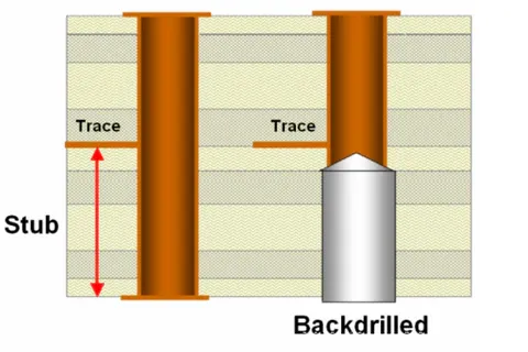
Back drilling, in simple terms, is a manufacturing process used to remove unused portions of plated-through-hole (PTH) vias, also known as stubs, to improve signal performance in high-speed circuits. Now, let’s explore every aspect of this technique to help you implement it effectively in your designs.
What Is PCB Back Drilling and Why Does It Matter?
PCB back drilling is a specialized process in PCB manufacturing where a slightly larger drill is used to remove the conductive stub of a via that isn’t connected to any active signal path. These stubs, if left in place, can cause signal reflections and degrade performance, especially in high-speed applications operating at frequencies above 1 GHz.
Imagine a signal traveling through a via on a multilayer PCB. If the via extends beyond the layers it connects, the unused portion (the stub) acts like an antenna, causing interference. By back drilling, you eliminate this stub, reducing signal loss and improving impedance matching. For instance, in a 10-layer board, if a via only connects layers 1 to 4, back drilling removes the conductive material from layers 5 to 10, ensuring cleaner signal transmission.
The Importance of Back Drilling in High-Speed Designs
In high-speed PCB designs, signal integrity is everything. As data rates increase—think 10 Gbps or higher—even small imperfections can lead to significant issues like crosstalk or signal distortion. Back drilling addresses this by minimizing the stub length, which directly impacts the impedance. For example, a stub length of just 0.5 mm can introduce a noticeable reflection in a signal operating at 5 GHz.
By adopting back drilling, you can achieve better control over impedance, often targeting a standard value like 50 ohms for single-ended signals or 100 ohms for differential pairs. This process is particularly vital for industries like telecommunications, aerospace, and data centers, where high-frequency signals are the norm.
Back Drilling Design Rules: Key Guidelines for Success
Designing a PCB with back drilling in mind requires careful planning. Following specific back drilling design rules ensures the process is effective and manufacturable. Here are the critical guidelines to consider:
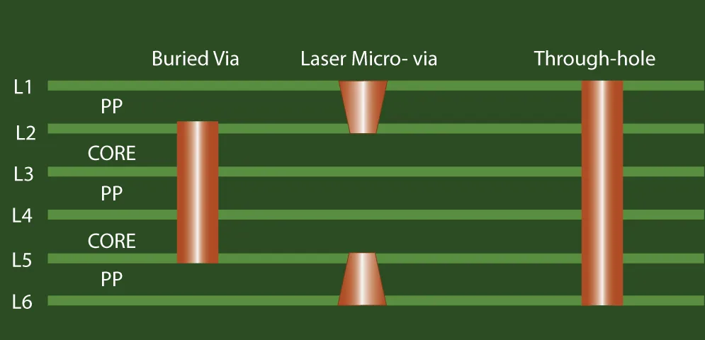
- Via Placement and Layer Planning: Identify which vias need back drilling early in the design phase. Typically, vias connecting only a subset of layers in a multilayer board are candidates. Ensure your design software marks these vias for back drilling.
- Stub Length Tolerance: Aim to keep the remaining stub length after back drilling as short as possible, ideally less than 0.25 mm for signals above 2.5 GHz. This minimizes signal reflection risks.
- Drill Size Accuracy: The back drill diameter should be slightly larger than the original via drill size, typically by 0.1 to 0.2 mm, to remove the conductive plating without damaging the via’s functional part.
- Aspect Ratio Consideration: Maintain a reasonable aspect ratio (board thickness to drill diameter) for back drilling, often below 10:1, to ensure precision and avoid drill breakage.
- Clear Documentation: Provide explicit instructions in your fabrication files, including which vias require back drilling and the target depth. Ambiguity can lead to manufacturing errors.
Following these rules during the design phase sets the foundation for a smooth manufacturing process and optimal performance.
Back Drilling Manufacturing: How It’s Done
The back drilling manufacturing process is a precision task that occurs after the initial drilling and plating of vias in PCB production. Here’s a step-by-step look at how it works:
- Initial Via Drilling and Plating: The PCB undergoes standard drilling to create vias, followed by plating to make them conductive across all layers.
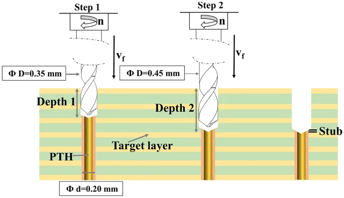
- Back Drilling Setup: A CNC drilling machine is programmed with the specific vias marked for back drilling. The drill bit used is slightly larger than the original via drill size—often by 0.15 mm—to ensure complete removal of the stub.
- Depth Control: The drilling depth is carefully controlled to stop just before the active signal layers. Advanced machines use sensors to detect layer transitions, achieving depth accuracy within 0.05 mm.
- Inspection: Post-drilling, the board is inspected using X-ray or other methods to confirm that stubs are removed without damaging functional via sections.
- Cleaning: Any debris from back drilling is cleaned to prevent contamination or shorts during subsequent assembly steps.
Precision is paramount in this process. A deviation of even 0.1 mm in depth can compromise signal paths or leave residual stubs, negating the benefits of back drilling. Manufacturers often test a sample board before full production to validate the setup.
Via Drill Size: Choosing the Right Dimensions
Selecting the appropriate via drill size is a critical factor in back drilling. The original via size and the back drill size must be carefully matched to ensure functionality and manufacturability. Here are key points to consider:
- Standard Via Sizes: Common via drill sizes range from 0.2 mm to 0.8 mm, depending on the board’s design and current-carrying requirements. Smaller vias are often used in high-density designs.
- Back Drill Size Increment: As a rule, the back drill should be 0.1 to 0.2 mm larger than the original via to remove the plated stub without affecting the via’s integrity. For example, a 0.3 mm via might use a 0.45 mm back drill.
- Manufacturer Capabilities: Confirm with your fabrication partner the minimum and maximum drill sizes they support for back drilling. Some may have limitations based on equipment or board thickness.
- Signal Integrity Impact: Smaller vias and back drills reduce parasitic capacitance, which is beneficial for high-speed signals. However, they increase manufacturing complexity and cost.
Balancing these factors ensures that your vias support both performance and production requirements. Always include detailed notes on drill sizes in your design files to avoid miscommunication.
PCB Troubleshooting Guide: Common Back Drilling Issues and Solutions
Even with careful planning, issues can arise during the PCB back drilling process. This PCB troubleshooting guide covers common problems and practical solutions to keep your project on track:
1. Incomplete Stub Removal
Problem: Residual stubs remain after back drilling, causing signal reflections. This often happens due to incorrect depth settings or drill wear.
Solution: Verify the back drill depth in your design files and ensure the manufacturer uses up-to-date drill bits. Post-process X-ray inspection can detect leftover stubs, allowing for rework if needed.
2. Damage to Functional Via Sections
Problem: Over-drilling damages the active part of the via, breaking signal connections. This can occur if depth control is imprecise.
Solution: Use manufacturers with advanced depth-sensing equipment. Specify a safety margin (e.g., 0.1 mm) above the last active layer to prevent over-drilling. Test a prototype before full production.
3. Misalignment of Back Drills
Problem: The back drill misses the via center, leaving partial stubs or creating unintended shorts.
Solution: Ensure your design files include precise via coordinates. Work with a fabricator that uses high-accuracy CNC machines, and request alignment checks during setup.
4. Increased Manufacturing Costs
Problem: Back drilling adds significant cost, especially for complex boards with many vias.
Solution: Optimize your design to minimize the number of vias requiring back drilling. Group vias in similar locations to streamline the process, reducing setup time.
Benefits and Challenges of PCB Back Drilling
Benefits
- Enhanced Signal Integrity: Eliminates stub-induced reflections, ensuring cleaner signals at high frequencies (e.g., above 2 GHz).
- Improved Impedance Control: Achieves tighter impedance matching, critical for differential pairs at 100 ohms.
- Support for High-Speed Applications: Enables reliable performance in cutting-edge designs like 5G or server boards.
Challenges
- Higher Costs: Back drilling adds expense due to additional manufacturing steps and precision requirements.
- Design Complexity: Requires meticulous planning and documentation to avoid errors.
- Manufacturing Limitations: Not all fabricators offer back drilling, and capabilities vary widely.
Best Practices for Implementing Back Drilling
To maximize the benefits of back drilling while minimizing challenges, follow these best practices:
- Collaborate closely with your fabrication partner during the design phase to align on capabilities and constraints.
- Use simulation tools to model signal integrity before and after back drilling to predict performance gains.
- Start with a prototype run to validate the back drilling process before committing to full-scale production.
- Regularly update your design guidelines based on feedback from manufacturing and testing phases.
Conclusion: Mastering PCB Back Drilling for Optimal Results
Back drilling is a powerful technique for enhancing the performance of high-speed PCBs by eliminating via stubs and improving signal integrity. By adhering to back drilling design rules, understanding the back drilling manufacturing process, selecting the right via drill size, and leveraging this PCB troubleshooting guide, you can tackle the challenges of modern PCB design with confidence.
Whether you’re working on telecommunications equipment, data center hardware, or other high-frequency applications, mastering the PCB back drilling process is a game-changer. With careful planning and execution, you can achieve superior signal quality and reliability in your designs. Equip yourself with these insights, and take your PCB projects to the next level.


