ALLPCB


In the fast-paced world of electronics, high-speed printed circuit boards (PCBs) are the backbone of modern devices. However, as signal speeds increase, maintaining signal quality becomes a challenge. This is where PCB back drilling comes into play. If you're wondering how to enhance signal integrity in high-frequency PCB design, back drilling is a powerful technique that reduces signal reflection, improves impedance matching, and optimizes vias. In this comprehensive guide, we'll break down the benefits of PCB back drilling, explore its role in high-speed designs, and provide actionable insights for engineers looking to elevate their PCB performance.
What Is PCB Back Drilling and Why Does It Matter?
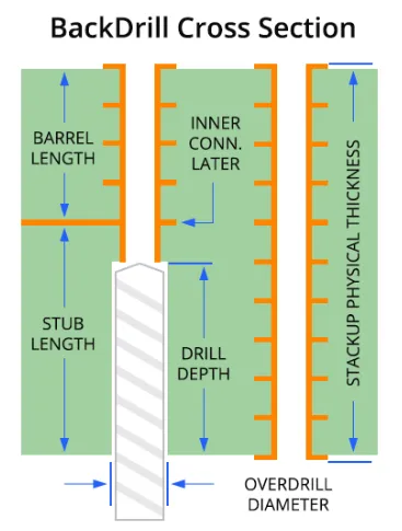
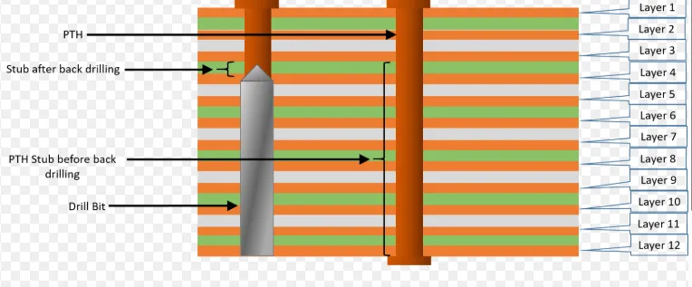
PCB back drilling, also known as controlled depth drilling or counterboring, is a specialized manufacturing process used in high-speed PCB design. It involves drilling a larger hole over an existing plated-through-hole (PTH) via to remove the unused portion of the via stub. A via stub is the section of the via that extends beyond the signal layer it connects to, and it can cause unwanted signal distortions in high-frequency applications.
Why does this matter? In high-speed boards, where signals operate at frequencies above 1 GHz, even small imperfections can lead to significant issues like signal reflection and impedance mismatches. Back drilling eliminates these stubs, ensuring cleaner signal transmission and better overall performance. This technique is especially critical for applications like 5G technology, radar systems, and high-performance servers, where signal integrity is non-negotiable.
The Key Benefits of PCB Back Drilling
Back drilling offers several advantages for engineers working on high-frequency PCB design. Let's dive into the most significant PCB back drilling benefits and how they impact performance.
1. Signal Reflection Reduction
In high-speed designs, via stubs act like tiny antennas, reflecting signals back into the transmission path. This reflection can cause interference, leading to data errors or signal loss. For example, at frequencies above 2.5 GHz, a via stub as short as 0.5 mm can introduce noticeable signal distortion. Back drilling removes these stubs, reducing reflections by up to 50% in some cases, ensuring that signals travel smoothly without interference.
2. Improved Impedance Matching
Impedance matching is critical for maintaining signal integrity in high-speed circuits. Via stubs disrupt the characteristic impedance of a trace, often deviating it from the standard 50 ohms used in many high-frequency designs. This mismatch can degrade signal quality. By eliminating the stub through back drilling, the impedance remains consistent across the signal path, minimizing losses and ensuring reliable data transfer.
3. Via Optimization for High-Speed Signals
Vias are essential for connecting different layers in a PCB, but unused stub portions create parasitic capacitance and inductance, which slow down signal transitions. Back drilling optimizes vias by removing these unnecessary sections, reducing parasitic effects and allowing signals to propagate faster. This is particularly important for designs with data rates exceeding 10 Gbps, where every nanosecond counts.
4. Enhanced Signal Integrity for High-Frequency PCB Design
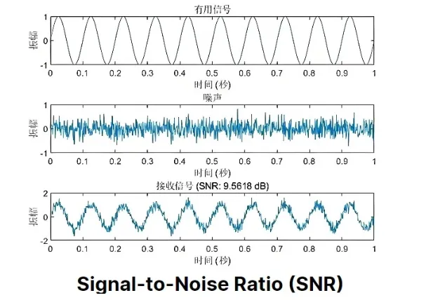
High-frequency PCB design demands pristine signal integrity to prevent errors in applications like telecommunications and data centers. Back drilling directly addresses issues like crosstalk and electromagnetic interference (EMI) by cleaning up the signal path. Studies have shown that back-drilled vias can improve signal-to-noise ratios by as much as 3 dB in high-speed systems, making this technique a game-changer for engineers.
How Does PCB Back Drilling Work?
Understanding the back drilling process is key to appreciating its value in high-frequency PCB design. Here's a step-by-step look at how it’s done:
- Design Planning: During the PCB layout phase, engineers identify vias that require back drilling based on signal paths and layer connections. Only vias with unused stubs in high-speed signal paths are targeted.
- Initial Drilling: Standard PTH vias are drilled and plated as part of the regular PCB manufacturing process.
- Controlled Depth Drilling: A larger drill bit, typically 0.2 mm wider than the original via, is used to remove the unused stub from the opposite side of the board. The depth is precisely controlled to avoid damaging the active signal layers.
- Inspection: After back drilling, the board undergoes inspection to ensure the stub has been removed without affecting the via's functionality or the PCB's structural integrity.
This process requires advanced equipment and precise control, as errors in depth or alignment can damage the board. Modern manufacturing facilities use automated drilling systems with depth accuracy within 0.05 mm to achieve consistent results.
Applications of Back Drilling in High-Frequency PCB Design
Back drilling is not a one-size-fits-all solution; it’s specifically tailored for high-speed and high-frequency applications. Here are some key areas where it delivers significant value:
- 5G Technology: With signal frequencies reaching up to 28 GHz in 5G networks, back drilling ensures minimal signal loss and reflection in base station hardware and mobile devices.
- Data Centers and Servers: High-speed servers handling data rates of 25 Gbps or higher rely on back drilling to maintain signal clarity across densely packed multilayer boards.
- Radar and Aerospace: Radar systems operating at high frequencies require pristine signal paths for accurate detection. Back drilling reduces noise, enhancing system reliability.
- Telecommunications: Back drilling supports high-speed communication equipment by optimizing vias and ensuring impedance matching for consistent performance.
Challenges and Considerations in PCB Back Drilling
While back drilling offers substantial benefits, it’s not without challenges. Engineers must consider the following factors when incorporating this technique into their designs:
1. Increased Manufacturing Complexity
Back drilling adds an extra step to the PCB fabrication process, requiring specialized equipment and skilled operators. This can increase production time and costs, especially for complex multilayer boards with numerous vias. For instance, a 16-layer board with hundreds of high-speed vias might require multiple drilling passes, adding hours to the manufacturing timeline.
2. Design Precision
Accurate design files are crucial for successful back drilling. Engineers must clearly specify which vias need drilling and at what depth. Errors in the design file can lead to over-drilling, damaging functional parts of the via, or under-drilling, leaving residual stubs. Using advanced PCB design software with 3D modeling capabilities can help visualize and verify back drilling requirements before fabrication.
3. Board Thickness and Material Constraints
Back drilling is most effective on thicker boards (above 2 mm) where via stubs are longer and more likely to cause issues. On thinner boards, the stub length may be negligible, making back drilling unnecessary. Additionally, the PCB material must withstand the drilling process without cracking or delaminating. High-quality laminates with good thermal and mechanical stability are recommended.
Best Practices for Implementing Back Drilling in High-Speed Designs
To maximize the benefits of back drilling while minimizing challenges, follow these best practices:
- Prioritize Critical Vias: Focus back drilling on vias associated with high-speed signals (above 1 GHz) to optimize cost and manufacturing time. Low-speed or power vias often don’t require this treatment.
- Collaborate with Fabricators Early: Work closely with your PCB manufacturer during the design phase to ensure they can meet back drilling specifications. Provide detailed documentation, including layer stack-up and drilling depths.
- Simulate Signal Performance: Use signal integrity simulation tools to model the impact of via stubs before and after back drilling. This helps validate the need for back drilling and fine-tune the design for impedance matching.
- Balance Cost and Performance: While back drilling improves signal quality, it’s not always necessary for every project. Evaluate the frequency and data rate requirements of your design to determine if the added cost is justified.
Future Trends: The Role of Back Drilling in Evolving Technologies
As electronics continue to evolve, the demand for high-speed and high-frequency PCB design will only grow. Emerging technologies like 6G, artificial intelligence hardware, and autonomous vehicles will push signal speeds beyond current limits, making techniques like back drilling even more essential. Additionally, advancements in manufacturing, such as laser-based back drilling, promise to improve precision and reduce costs, making this technique accessible for a broader range of applications.
Moreover, the integration of back drilling with other signal integrity solutions, like optimized trace routing and advanced materials, will create a holistic approach to PCB design. Engineers who stay ahead of these trends will be well-positioned to tackle the challenges of next-generation electronics.
Conclusion: Elevate Your High-Speed Designs with PCB Back Drilling
PCB back drilling is a proven technique for improving signal quality in high-speed boards, offering benefits like signal reflection reduction, impedance matching, and via optimization. By removing unused via stubs, it ensures cleaner signal paths, making it indispensable for high-frequency PCB design in applications ranging from 5G to data centers. While it introduces some manufacturing complexity, the performance gains often outweigh the challenges, especially for cutting-edge projects.
By understanding the process, benefits, and best practices of back drilling, engineers can make informed decisions to enhance their designs. Whether you're working on a telecommunications system or a high-performance server, incorporating back drilling can be the key to achieving superior signal integrity and reliability. Embrace this technique to stay competitive in the ever-evolving world of electronics design.