 ALLPCB


In the fast-paced world of electronics, designing a printed circuit board (PCB) that performs at its best is crucial. One of the most effective ways to achieve this is through PCB stack-up design sequential build-up. But what exactly does this mean, and how can it improve your PCB performance? In short, sequential build-up (SBU) is a method of constructing multilayer PCBs by adding layers step by step, allowing for intricate designs, better signal integrity, and optimized performance. This blog will explore the ins and outs of sequential build-up PCB layer arrangement, the right sequential build-up PCB materials, and essential sequential build-up PCB design rules to help you create high-performing boards.
Whether you're an engineer working on high-speed designs or a designer looking to improve reliability, this guide will walk you through actionable tips and detailed insights. Let's dive into the world of sequential build-up stack-up design and see how it can elevate your PCB projects.
What is Sequential Build-Up in PCB Stack-Up Design?
Sequential build-up, often abbreviated as SBU, is a manufacturing technique used to create multilayer PCBs. Unlike traditional methods where all layers are laminated together in one step, SBU involves adding layers one at a time or in small groups. This process allows for greater control over the board's structure, enabling designers to incorporate features like microvias and buried vias that are essential for high-density interconnect (HDI) designs.
The primary advantage of PCB stack-up design sequential build-up is its ability to support complex designs in compact spaces. As electronic devices become smaller and more powerful, the demand for multilayer PCBs with precise layer arrangements has skyrocketed. SBU meets this need by allowing engineers to build boards with 8, 10, or even 14 layers while maintaining signal integrity and reducing electromagnetic interference (EMI).
Why Choose Sequential Build-Up for PCB Performance?
Sequential build-up offers several benefits that directly impact PCB performance. Here are the key reasons why this method stands out:
- Improved Signal Integrity: By carefully arranging layers and using microvias, SBU reduces signal loss and crosstalk, which is critical for high-speed designs operating at frequencies above 1 GHz.
- Compact Designs: SBU enables the use of HDI technology, allowing more components to fit into smaller spaces without sacrificing performance.
- Better Thermal Management: With precise control over layer placement, heat dissipation can be optimized by placing power and ground planes strategically.
- Cost Efficiency in Complex Designs: While SBU can be more expensive than traditional methods for simple boards, it saves costs in high-layer-count designs by reducing the need for additional connectors or boards.
For example, in a 10-layer PCB designed for a high-speed communication device, using SBU can help maintain a controlled impedance of 50 ohms across critical signal layers, ensuring minimal signal distortion.
Understanding Sequential Build-Up PCB Layer Arrangement
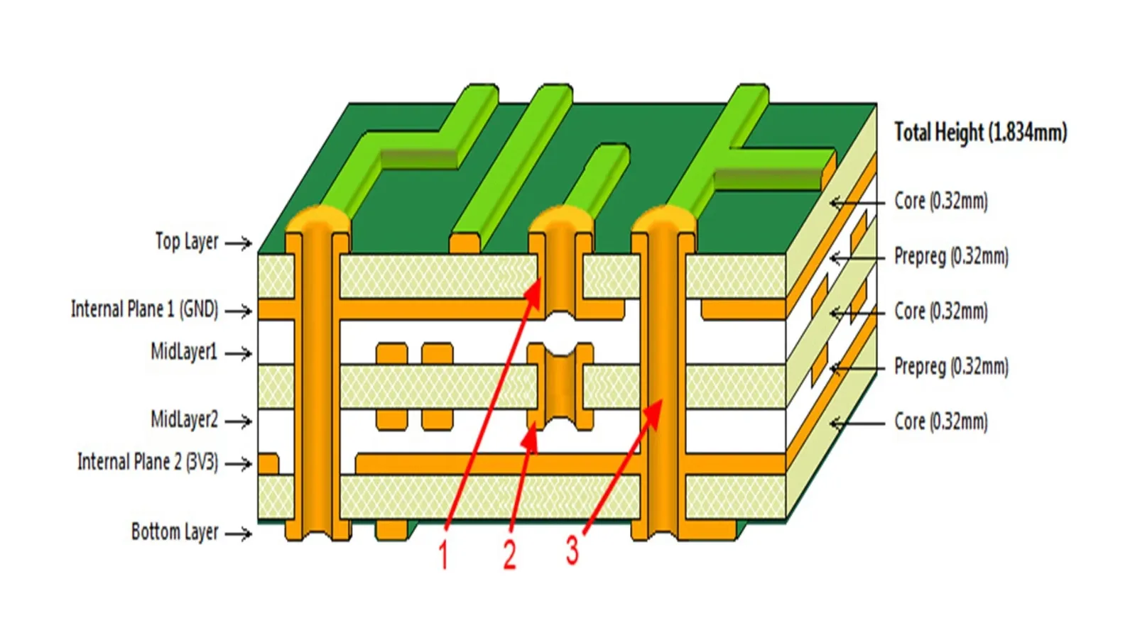
The sequential build-up PCB layer arrangement is at the heart of optimizing performance. The way layers are stacked and connected plays a huge role in how well the board handles signals, power distribution, and noise. Here's a breakdown of how to approach layer arrangement with SBU:
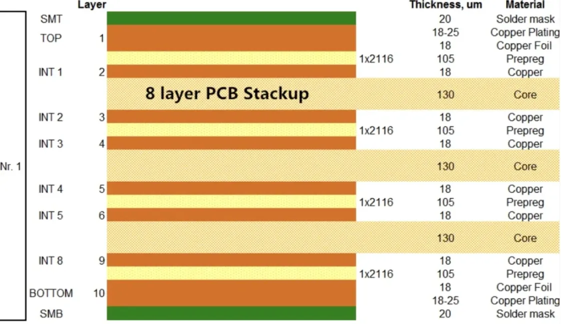
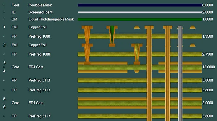
- Start with Core Layers: The process often begins with a core layer, which is a thin, rigid base. Additional layers are built on top of this core through lamination and drilling processes.
- Add Signal and Power Layers: Signal layers are typically placed near the surface for easy access, while power and ground planes are positioned in the middle to reduce EMI and provide stable voltage distribution.
- Incorporate Vias: Microvias and buried vias are added during the build-up process to connect layers without taking up too much space. For instance, a microvia with a diameter of 0.1 mm can connect adjacent layers in an HDI design.
- Balance Symmetry: To prevent warping during manufacturing, ensure the stack-up is symmetrical. For a 12-layer board, this might mean having equal numbers of layers above and below the core.
A common arrangement for an 8-layer SBU PCB might look like this: Signal (Top), Ground, Signal, Power, Power, Signal, Ground, Signal (Bottom). This setup ensures that high-speed signals are shielded by ground planes to minimize interference.
Choosing the Right Sequential Build-Up PCB Materials
Selecting the appropriate sequential build-up PCB materials is just as important as the layer arrangement. The materials used in SBU directly affect the board's electrical performance, thermal stability, and durability. Here's what to consider:
- Dielectric Materials: High-frequency designs often use low-loss dielectric materials with a dielectric constant (Dk) between 3.0 and 4.0 to maintain signal integrity. For standard applications, FR-4 with a Dk of around 4.5 is a cost-effective choice.
- Copper Thickness: Copper layers in SBU designs typically range from 0.5 oz to 2 oz per square foot. Thicker copper (e.g., 2 oz) is ideal for power planes to handle higher currents, while thinner copper (e.g., 0.5 oz) works well for signal layers.
- Prepreg and Core: Prepreg (pre-impregnated resin) layers bond the core and build-up layers together. Choosing a prepreg with a similar thermal expansion coefficient to the core prevents delamination during temperature changes.
- High-Temperature Materials: For applications exposed to harsh environments, materials with a high glass transition temperature (Tg), such as 170°C or above, ensure reliability.
For a high-speed design operating at 5 GHz, using a low-loss dielectric material with a dissipation factor (Df) of 0.002 or lower can significantly reduce signal attenuation compared to standard FR-4.
Essential Sequential Build-Up PCB Design Rules
Following strict sequential build-up PCB design rules ensures that your board is manufacturable and performs as intended. These rules cover everything from layer spacing to via placement. Here are the most critical guidelines:
- Control Impedance: Maintain consistent impedance across signal layers by calculating trace widths and dielectric thicknesses. For a 50-ohm impedance, a trace width of 6 mils on a 4-mil dielectric layer is often ideal, though this varies based on materials.
- Minimize Via Stub Lengths: Long via stubs can cause signal reflections. Use back-drilling or microvias to keep stub lengths under 10 mils for high-speed signals.
- Plane Spacing: Keep power and ground planes close together (e.g., 3-5 mils apart) to create a low-inductance path for return currents, reducing EMI.
- Layer Thickness Consistency: Ensure uniform layer thicknesses during build-up to avoid stress points. A typical dielectric thickness between layers might be 4-8 mils, depending on the design.
- Avoid Overlapping Vias: Stagger vias in HDI designs to prevent structural weaknesses. Maintain a minimum spacing of 8 mils between microvias in adjacent layers.
By adhering to these rules, you can avoid common issues like signal crosstalk, which can degrade performance in boards operating at speeds above 500 MHz, or manufacturing defects that lead to costly reworks.
Challenges in Sequential Build-Up Stack-Up Design
While SBU offers many advantages, it also comes with challenges that designers must navigate. Understanding these hurdles can help you plan better and avoid pitfalls:
- Manufacturing Complexity: Adding layers sequentially requires precise alignment and lamination, increasing production time and cost for boards with 10 or more layers.
- Thermal Stress: Repeated lamination cycles in SBU can introduce thermal stress, potentially causing delamination if materials aren't matched properly.
- Signal Integrity Issues: Without careful planning, high-density designs can suffer from crosstalk or impedance mismatches, especially at frequencies above 2 GHz.
To mitigate these issues, work closely with your manufacturing partner to ensure they can handle the specific requirements of SBU designs, such as microvia drilling accuracy to within 0.05 mm.
Best Practices for Optimizing PCB Performance with SBU
To get the most out of PCB stack-up design sequential build-up, follow these best practices tailored for engineers and designers:
- Use Simulation Tools: Before finalizing your design, simulate the stack-up to predict signal behavior and thermal performance. This can help identify issues like a 10% impedance mismatch before manufacturing.
- Prioritize Ground Planes: Place ground planes adjacent to signal layers to provide a return path and reduce noise. For a 6-layer board, aim for at least two ground planes.
- Test Prototypes: Build and test a small batch of prototypes to validate your design rules and material choices under real-world conditions.
- Document Everything: Keep detailed records of layer arrangements, material specs, and design rules to streamline future projects or troubleshooting.
Conclusion: Elevate Your PCB Designs with Sequential Build-Up
Mastering sequential build-up PCB layer arrangement, choosing the right sequential build-up PCB materials, and following sequential build-up PCB design rules can transform your PCB projects. The sequential build-up method empowers you to create compact, high-performance boards that meet the demands of modern electronics, from high-speed communication devices to intricate IoT gadgets.
By focusing on precise layer stacking, material selection, and adherence to design guidelines, you can minimize issues like EMI, signal loss, and manufacturing defects. The result is a reliable, efficient PCB that performs at its peak, no matter the application. Start incorporating these strategies into your next design, and watch as your boards reach new levels of performance and reliability.


