 ALLPCB


In the world of electronics, ensuring high-quality signal transmission is vital, especially for high-frequency designs. One critical factor that often gets overlooked is PCB lamination and its direct impact on signal integrity. Poor lamination choices can lead to signal loss, impedance mismatch, and degraded performance. So, how does PCB lamination affect signal integrity, and what can you do to minimize loss while maximizing performance? In this comprehensive guide, we’ll explore the relationship between PCB lamination, signal integrity, dielectric constants, and high-frequency signals, offering practical tips to optimize your PCB design.
What is PCB Lamination and Why Does It Matter?
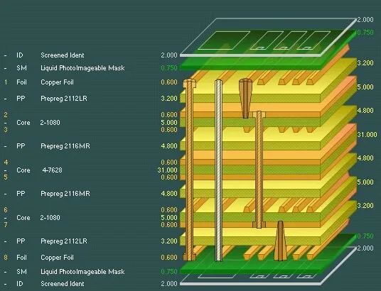
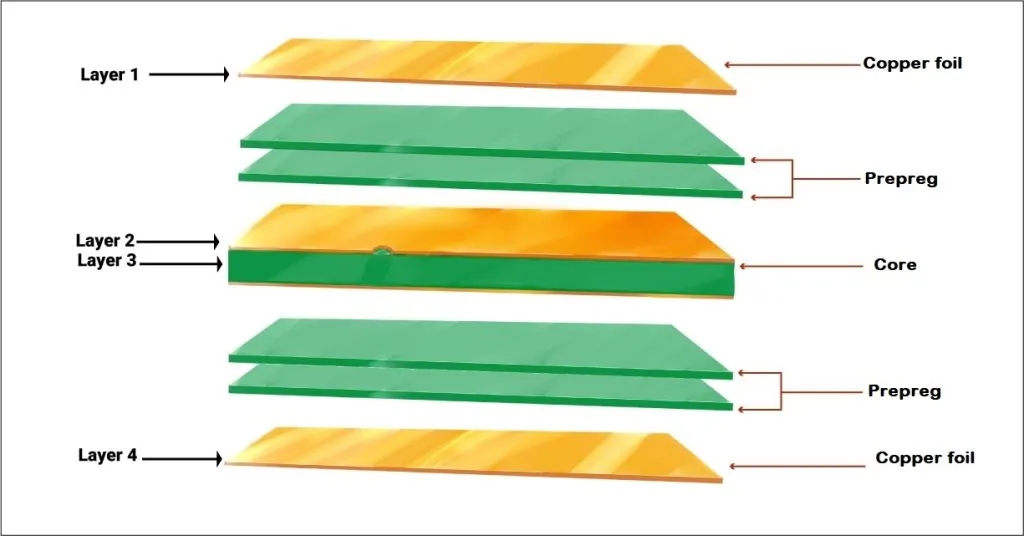
PCB lamination is the process of bonding multiple layers of materials together to form a printed circuit board. These layers typically include conductive copper traces and insulating dielectric materials, which are pressed together under heat and pressure. The quality and properties of these materials, as well as the lamination process itself, play a significant role in determining how well signals travel through the board.
For high-frequency signals—those operating at gigahertz ranges—even small variations in the lamination process can cause issues like signal loss or impedance mismatch. Signal integrity, which refers to the ability of a signal to maintain its shape and timing as it travels through the PCB, depends heavily on consistent material properties and precise manufacturing. A poorly laminated PCB can introduce noise, crosstalk, or delays, leading to system failures in applications like telecommunications, automotive radar, or high-speed computing.
Understanding Signal Integrity in PCB Design
Signal integrity is the foundation of reliable electronic performance. It ensures that a signal sent from one point on a PCB reaches its destination without distortion. Factors like signal loss, reflections, and crosstalk can degrade signal integrity, especially in high-frequency designs where timing and precision are critical.
In high-frequency applications, signals travel at speeds close to the speed of light, and even tiny inconsistencies in the PCB can cause problems. For example, a signal operating at 5 GHz has a wavelength of about 60 mm in a typical dielectric material. If the PCB’s dielectric constant varies by just 0.1 across the board, it can shift the signal’s timing by picoseconds, enough to cause errors in data transmission.
PCB lamination impacts signal integrity by influencing the uniformity of the dielectric material and the alignment of layers. Let’s dive deeper into the specific ways lamination affects performance.
How PCB Lamination Impacts Signal Integrity
1. Dielectric Constant Variations
The dielectric constant (Dk) of a PCB material determines how fast a signal travels through it and how much energy is stored in the electric field. Materials with a higher Dk slow down signals, while those with a lower Dk allow faster transmission. During lamination, if the dielectric material isn’t uniform or if air bubbles are trapped between layers, the Dk can vary across the board. This inconsistency causes signals to travel at different speeds in different areas, leading to timing errors and signal loss.
For high-frequency signals, choosing a material with a stable and low Dk is crucial. Common materials like FR-4 have a Dk of around 4.3 to 4.5, which is suitable for lower frequencies but may introduce losses at higher frequencies (above 1 GHz). Specialized laminates with Dk values closer to 3.0 or lower are often used in high-speed designs to minimize these effects.
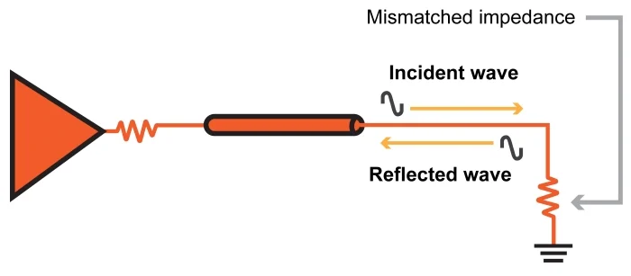
2. Impedance Mismatch Due to Lamination Issues
Impedance mismatch occurs when the characteristic impedance of a transmission line doesn’t match the load or source impedance, causing signal reflections. In PCB design, impedance is controlled by the trace width, trace spacing, and the dielectric thickness between layers. During lamination, if the dielectric layers are not evenly pressed or if there’s a mismatch in material properties, the impedance can vary across the board.
For example, a typical high-speed design might target a 50-ohm impedance for transmission lines. If the dielectric thickness varies by even 0.1 mm due to poor lamination, the impedance could shift by several ohms, leading to reflections and signal degradation. Maintaining tight control over the lamination process ensures that the dielectric thickness remains consistent, preserving impedance and reducing signal loss.
3. Signal Loss from Material Dissipation
Signal loss, often measured as insertion loss, happens when a signal loses energy as it travels through the PCB. A key factor in this loss is the dissipation factor (Df) of the dielectric material used in lamination. Materials with a high Df absorb more signal energy, converting it into heat, which is especially problematic for high-frequency signals.
During lamination, the choice of material and the quality of bonding affect how much signal loss occurs. For instance, FR-4 materials typically have a Df of 0.02, which is acceptable for low-frequency designs but causes significant loss at frequencies above 5 GHz. High-performance laminates with a Df of 0.002 or lower are better suited for minimizing loss in high-frequency applications.
4. Layer Misalignment and Crosstalk
In multilayer PCBs, lamination must ensure precise alignment of copper traces and dielectric layers. If layers shift during the lamination process, it can lead to misalignment of traces, increasing the risk of crosstalk—unwanted coupling of signals between adjacent traces. Crosstalk is particularly problematic for high-frequency signals, as it introduces noise and distorts the signal waveform.
Proper lamination techniques, such as controlled pressure and temperature during bonding, help prevent layer misalignment and maintain signal integrity across the board.
Strategies to Minimize Signal Loss and Maximize Performance
Now that we understand how PCB lamination impacts signal integrity, let’s explore actionable strategies to minimize signal loss and optimize performance in high-frequency PCB designs.
1. Choose the Right Dielectric Material
Selecting a dielectric material with a low and stable dielectric constant (Dk) and low dissipation factor (Df) is critical for high-frequency designs. For applications operating above 1 GHz, consider using advanced laminates designed for low loss. These materials maintain consistent Dk values (often between 2.2 and 3.5) and have Df values as low as 0.001, reducing signal loss significantly compared to standard materials like FR-4.
Additionally, ensure that the chosen material is compatible with your lamination process to avoid issues like delamination or uneven bonding.
2. Control Dielectric Thickness for Impedance Matching
Impedance matching is essential for preventing signal reflections. Work closely with your PCB manufacturer to specify tight tolerances for dielectric thickness during lamination. For a 50-ohm transmission line, even a 10% variation in dielectric thickness can cause a measurable impedance mismatch. Use simulation tools to calculate the exact trace width and dielectric thickness needed for your design, and verify these parameters after lamination.
3. Optimize the Lamination Process
The lamination process itself must be carefully controlled to avoid defects like air bubbles, uneven pressure, or temperature variations. These issues can lead to inconsistent dielectric properties and poor layer bonding. Partner with a manufacturer that uses advanced lamination equipment and follows strict quality control measures to ensure uniformity across the board.
4. Use Ground Planes to Reduce Crosstalk
In multilayer PCBs, incorporating solid ground planes between signal layers can significantly reduce crosstalk and improve signal integrity. During lamination, ensure that ground planes are properly aligned and bonded to avoid gaps that could introduce noise. A well-designed ground plane also helps maintain consistent impedance for high-frequency signals.
5. Test and Validate Your Design
After lamination, perform thorough testing to validate signal integrity. Use tools like Time Domain Reflectometry (TDR) to measure impedance across transmission lines and identify any mismatches caused by lamination issues. Additionally, test for insertion loss and crosstalk to ensure that the board meets performance requirements for high-frequency signals.
Practical Examples of Lamination Impact in High-Frequency Designs
To illustrate the real-world impact of PCB lamination on signal integrity, let’s consider two scenarios.
Scenario 1: Telecommunications Equipment
A telecommunications device operating at 10 GHz requires minimal signal loss to maintain data rates. Using a standard FR-4 material with a Dk of 4.4 and Df of 0.02 results in an insertion loss of 0.5 dB per inch at 10 GHz, which is unacceptable for long traces. Switching to a high-performance laminate with a Dk of 3.0 and Df of 0.002 reduces the loss to 0.1 dB per inch, significantly improving performance.
Scenario 2: Automotive Radar System
An automotive radar system operating at 77 GHz is highly sensitive to impedance mismatch. A lamination defect causes a 0.2 mm variation in dielectric thickness, shifting the impedance of a critical transmission line from 50 ohms to 55 ohms. This mismatch leads to a 10% signal reflection, causing errors in radar detection. Tightening lamination tolerances to within 0.05 mm resolves the issue and restores performance.
Conclusion: Prioritizing Lamination for Signal Integrity
PCB lamination is a critical yet often underestimated factor in maintaining signal integrity, especially for high-frequency signals. Variations in dielectric constant, impedance mismatch, signal loss, and layer misalignment can all stem from poor lamination practices, leading to degraded performance and system failures. By choosing the right materials, controlling dielectric thickness, optimizing the lamination process, and validating designs through testing, you can minimize signal loss and maximize performance in your PCB designs.
Whether you’re working on telecommunications equipment, automotive systems, or high-speed computing, paying attention to lamination details ensures that your signals remain clear and reliable. With the right approach, you can tackle the challenges of high-frequency PCB design and achieve outstanding results.


