 ALLPCB


In the fast-paced world of electronics, signal integrity is everything. If you're dealing with high-speed designs, via stubs can be a silent killer, causing signal reflections and degrading performance. So, how do you eliminate them? Backdrilling in PCB manufacturing is the answer. This process, also known as controlled depth drilling, removes unused portions of through-hole vias to improve signal quality. In this comprehensive guide, we'll dive deep into the backdrilling PCB manufacturing process, explore controlled depth drilling techniques, discuss back drilling equipment, and provide a practical PCB via drilling tutorial with design for manufacturing (DFM) tips for PCB back drilling. Let’s get started!
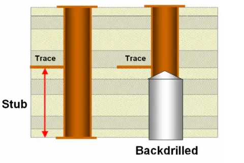
What Are Via Stubs and Why Do They Matter?
Vias are essential in multilayer printed circuit boards (PCBs) to connect different layers. However, in through-hole vias, a portion of the via often remains unused, creating what’s called a "via stub." This stub acts like a tiny antenna, causing signal reflections, noise, and crosstalk, especially in high-speed designs operating at frequencies above 1 GHz. For instance, a via stub as short as 0.5 mm can introduce significant signal distortion at 10 Gbps data rates, leading to impedance mismatches of up to 10-15 ohms.
Backdrilling addresses this by removing the unused stub, ensuring cleaner signal transmission. This technique is critical for applications like telecommunications, data centers, and high-speed computing, where even minor signal loss can lead to system failures.
Understanding the Backdrilling PCB Manufacturing Process
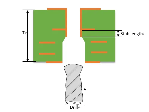
Backdrilling, also referred to as controlled depth drilling, is a precision technique used during PCB fabrication. It involves drilling a slightly larger hole from the opposite side of the board to remove the unused copper barrel of a via stub without affecting the functional part of the via. Here’s how the backdrilling PCB manufacturing process typically works:
- Design and Planning: The PCB design must specify which vias need backdrilling. This is often determined by signal integrity simulations that identify problematic stubs in high-speed signal paths.
- Initial Drilling: Standard through-hole vias are drilled and plated with copper to connect the layers as needed.
- Backdrilling Setup: Using specialized equipment, a larger drill bit (typically 0.2-0.3 mm wider than the original via) is aligned precisely with the target via.
- Controlled Depth Drilling: The drill removes the unused copper stub to a specific depth, leaving the functional via intact. Depth control is critical—modern machines achieve tolerances as tight as ±0.05 mm.
- Inspection: Post-drilling, the board is inspected using X-ray or automated optical inspection (AOI) to ensure accuracy and no damage to the functional via.
The result? A via with minimal stub length, reducing signal reflections and ensuring impedance continuity. For high-speed signals, this can improve signal integrity by up to 30%, depending on the design and frequency.
Controlled Depth Drilling: Precision at Its Core
Controlled depth drilling is the heart of backdrilling. This technique requires extreme accuracy to avoid damaging the PCB’s functional layers. Modern fabrication facilities use advanced CNC (Computer Numerical Control) machines equipped with depth-sensing technology to achieve this precision. Here are key aspects of controlled depth drilling:
- Depth Accuracy: Drilling depth must be controlled within tight tolerances, often ±0.025 mm, to ensure the stub is removed without cutting into the active signal path.
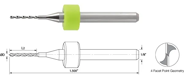
- Drill Bit Selection: A slightly larger drill bit is used to avoid damaging the via walls. For a 0.3 mm via, a 0.5-0.6 mm backdrill bit might be chosen.
- Layer Awareness: The drilling process must account for the exact layer stackup. Misalignment or over-drilling can sever critical connections, leading to board failure.
Controlled depth drilling is especially challenging in boards with 16 or more layers, where stackup complexity increases. However, with proper equipment and expertise, it’s a reliable way to enhance signal performance.
Back Drilling Equipment: Tools of the Trade
The success of backdrilling hinges on the quality of back drilling equipment. High-precision tools are non-negotiable for achieving the tight tolerances required. Here’s a look at the essential equipment used in the process:
- CNC Drilling Machines: These machines are the backbone of backdrilling, offering precise control over drill depth and alignment. Many modern systems can handle up to 20,000 RPM with positional accuracy of ±0.01 mm.
- Depth Control Sensors: Integrated sensors detect the drill’s depth in real-time, stopping at the programmed limit to prevent over-drilling.
- ility and ability to maintain sharpness during high-volume production.
- Inspection Tools: Post-drilling, X-ray machines and AOI systems verify the accuracy of stub removal and check for defects like misalignment or copper residue.
Investing in advanced back drilling equipment ensures repeatability and reliability, which are critical for high-speed PCB production. For engineers, collaborating with a manufacturer that prioritizes such technology can make all the difference in project outcomes.
PCB Via Drilling Tutorial: A Step-by-Step Guide
For engineers new to the concept, understanding how via drilling and backdrilling integrate into the PCB fabrication process is essential. This PCB via drilling tutorial focuses on the practical steps and considerations for incorporating backdrilling into your design workflow.
Step 1: Identify High-Speed Signals
Start by analyzing your PCB design to pinpoint vias associated with high-speed signals (e.g., above 1 GHz). Use signal integrity simulation tools to identify via stubs that could cause reflections or impedance mismatches.
Step 2: Specify Backdrilling in Design Files
Mark the vias requiring backdrilling in your design files. Clearly indicate the target depth and layers to be drilled. Most design software allows you to add notes or layers specifically for manufacturing instructions.
Step 3: Collaborate with Your Manufacturer
Share detailed stackup information and backdrilling requirements with your fabrication partner. Confirm their capability to achieve the necessary depth tolerances, especially for complex multilayer boards.
Step 4: Review DFM Guidelines
Ensure your design adheres to design for manufacturing (DFM) rules for backdrilling. This includes maintaining adequate spacing between vias (typically 0.8 mm minimum) to avoid drill interference and specifying via sizes compatible with backdrilling tools.
Step 5: Validate Post-Fabrication
After fabrication, request inspection reports or perform your own testing to verify stub removal. Tools like time-domain reflectometry (TDR) can measure impedance and confirm that signal integrity has improved.
By following these steps, you can seamlessly integrate backdrilling into your PCB projects, ensuring optimal performance for high-speed applications.
PCB Back Drilling DFM: Best Practices for Success
Design for manufacturing (DFM) is critical when incorporating backdrilling into your PCB layout. Poor design choices can lead to fabrication errors, increased costs, or compromised board reliability. Here are essential PCB back drilling DFM tips to keep in mind:
- Via Placement: Avoid placing vias too close to each other. A minimum spacing of 0.8-1.0 mm between vias prevents drill overlap and reduces the risk of structural damage during backdrilling.
- Layer Stackup Optimization: Design your stackup to minimize stub length naturally where possible. For example, route high-speed signals on outer layers to reduce the need for deep backdrilling.
- Specify Tolerances: Clearly define acceptable depth tolerances in your design files. A common range is ±0.05 mm, but this may vary based on board thickness and layer count.
- Avoid Overlapping Drills: Ensure backdrilled vias don’t interfere with nearby components or traces. Overlapping drills can weaken the board or cause unintended shorts.
- Test Points: Include test points in your design to measure signal integrity post-backdrilling. This helps validate the process and catch issues early.
Following these DFM guidelines not only ensures a smoother manufacturing process but also reduces costs by minimizing errors and rework. Always communicate with your fabrication team to align on specific capabilities and constraints.
Suggested Image Placement: Place a visual here showing a PCB layout with annotations for backdrilling DFM considerations like via spacing and depth. ALT Text: "PCB layout with DFM annotations for backdrilling via spacing and depth."
Benefits of Backdrilling in High-Speed PCB Designs
Backdrilling offers several advantages, particularly for high-speed and high-frequency applications. Here’s why it’s worth considering for your next project:
- Improved Signal Integrity: Removing via stubs reduces signal reflections, ensuring cleaner data transmission. This can lower bit error rates by up to 20% in systems running at 10 Gbps or higher.
- Reduced Crosstalk: Eliminating stubs minimizes electromagnetic interference between adjacent vias, which is critical in dense designs.
- Better Impedance Matching: Backdrilling helps maintain consistent impedance along signal paths, often bringing variations down to within ±5 ohms of the target value.
- Support for Higher Frequencies: As data rates climb beyond 25 Gbps, backdrilling becomes essential to meet performance standards in industries like 5G and cloud computing.
While backdrilling adds a step to the manufacturing process, the performance gains far outweigh the additional effort for critical applications.
Challenges and Limitations of Backdrilling
Despite its benefits, backdrilling isn’t without challenges. Understanding these limitations can help you make informed decisions during design and fabrication:
- Increased Costs: Backdrilling requires specialized equipment and additional processing time, which can increase fabrication costs by 10-20% compared to standard drilling.
- Design Complexity: Accurately specifying backdrilling requirements adds complexity to the design phase, requiring close collaboration with manufacturers.
- Board Thickness Constraints: Very thick boards (above 3.2 mm) or those with high layer counts (24+) can pose challenges for precise depth control.
- Potential for Errors: Misalignment or over-drilling can damage the board, necessitating rigorous quality control measures.
By weighing these challenges against the performance benefits, you can determine if backdrilling is the right choice for your project.
Conclusion: Mastering Backdrilling for Superior PCB Performance
Via stubs may be small, but their impact on high-speed PCB designs is anything but minor. Backdrilling in PCB manufacturing offers a proven solution to eliminate these stubs, ensuring cleaner signals, reduced noise, and better overall performance. By understanding the backdrilling PCB manufacturing process, leveraging controlled depth drilling techniques, selecting the right back drilling equipment, following a practical PCB via drilling tutorial, and adhering to PCB back drilling DFM best practices, you can optimize your designs for success.
Whether you’re working on telecommunications equipment, data center hardware, or cutting-edge consumer electronics, backdrilling is a tool worth mastering. With the insights and tips provided in this guide, you’re well-equipped to tackle via stubs head-on and deliver high-quality, reliable PCBs for even the most demanding applications.


