 ALLPCB


In the fast-evolving world of electronics, achieving higher density and better performance in printed circuit board (PCB) designs is crucial. One technology that stands out for addressing these needs is via-in-pad microvias, often used in high-density interconnect (HDI) PCB designs. If you're looking to optimize ball grid array (BGA) layouts with via-in-pad microvia or VIPPO (via-in-pad plated over) techniques, you're in the right place. This blog dives deep into how these technologies work, their benefits for BGA breakout, and key considerations like microvia impedance control. Let's explore how to maximize your PCB performance with these advanced solutions.
What Are Via-in-Pad Microvias and Why Do They Matter?
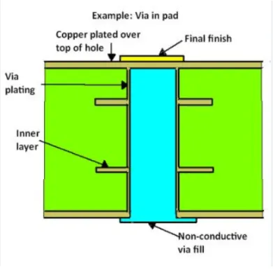
Via-in-pad microvias are small, laser-drilled holes placed directly within the pads of surface-mount components, such as BGAs. Unlike traditional vias that are positioned outside component pads, this approach saves valuable space on the PCB surface. These microvias, typically less than 150 micrometers in diameter, connect adjacent layers in an HDI PCB design, enabling compact layouts without sacrificing electrical performance.
For engineers working on BGA designs, via-in-pad microvias are a game-changer. They allow for tighter component spacing and more efficient routing, especially in devices where board real estate is limited, like smartphones, wearables, and medical equipment. By integrating vias into the pad, you reduce the need for additional surface traces, directly impacting signal integrity and overall design density.
Key Benefits of Via-in-Pad Microvias in BGA Designs
- Space Efficiency: Placing vias within pads eliminates the need for extra routing space, allowing for finer pitch BGAs (as low as 0.3mm) to be used effectively.
- Improved Signal Integrity: Shorter connection paths reduce parasitic inductance and capacitance, which is critical for high-speed signals operating at frequencies above 1 GHz.
- Enhanced Thermal Management: Direct via placement under components like BGAs can improve heat dissipation by creating shorter thermal paths to inner layers.
- Higher Component Density: With HDI PCB design, microvias enable stacking and sequential lamination, supporting more components per unit area.
Understanding VIPPO: Via-in-Pad Plated Over Technology
VIPPO, or via-in-pad plated over, is a specific manufacturing technique where the microvia within the pad is filled and plated over to create a flat surface. This process ensures that the pad remains smooth for reliable soldering of BGA components. Without VIPPO, an open via could lead to solder wicking, where solder flows into the via during assembly, causing weak joints or connection failures.
In BGA breakout designs, VIPPO is often preferred because it enhances manufacturing reliability. The plated-over via prevents air pockets or voids during reflow soldering, which is essential for maintaining consistent electrical and mechanical connections. This technology is particularly useful for fine-pitch BGAs, where even small soldering defects can lead to significant performance issues.
Advantages of VIPPO in HDI PCB Design
- Reliable Soldering: A flat pad surface ensures uniform solder application, reducing defects by up to 30% in high-density assemblies.
- Better Mechanical Strength: Filled vias provide additional structural support, minimizing the risk of pad damage during thermal cycling.
- Compatibility with Fine-Pitch Components: VIPPO supports pitches as low as 0.4mm, ideal for modern BGA packages.
BGA Breakout Challenges and How Via-in-Pad Microvias Help
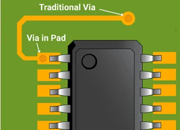
BGA breakout refers to the process of routing signals from the densely packed pins of a BGA component to other parts of the PCB. With traditional via placement, routing signals from a BGA with hundreds of pins (like a 400-pin package at 0.8mm pitch) often requires multiple layers and complex trace patterns. This not only increases board size but also risks signal crosstalk and impedance mismatches.
Via-in-pad microvias simplify BGA breakout by allowing direct connections beneath the component. Instead of routing traces outward to reach a via, signals can travel vertically through microvias to inner layers, reducing trace length by as much as 50% in some designs. This shorter path is vital for high-speed applications, where signal delays must be minimized to maintain data integrity at rates exceeding 10 Gbps.
Practical Example: Routing a 0.5mm Pitch BGA
Consider a 0.5mm pitch BGA with 256 pins. Using traditional vias, you might need to fan out traces across two or three layers, increasing the board footprint by 20-30%. With via-in-pad microvias, you can place vias directly under each pad, routing signals to inner layers immediately. This approach can reduce the required surface area by up to 40%, making it ideal for compact devices.
Microvia Impedance Control: Ensuring Signal Integrity
One critical aspect of using via-in-pad microvias in HDI PCB design is impedance control. Impedance mismatches in vias can cause signal reflections, leading to data loss or errors in high-speed circuits. Microvias, due to their smaller size, have lower parasitic effects compared to standard through-hole vias, but careful design is still necessary to maintain consistent impedance.
For instance, a typical microvia with a diameter of 100 micrometers and a depth of 0.25mm might contribute only 0.1nH of inductance, compared to 1.2nH for a standard via. However, if the via aspect ratio (depth-to-diameter) exceeds 1:1, signal degradation can occur due to increased resistance. To address this, designers must ensure proper via stacking and layer transitions in HDI builds.
Tips for Microvia Impedance Control
- Match Via Geometry: Keep the microvia diameter and depth proportional to maintain a target impedance, often around 50 ohms for high-speed signals.
- Use Back-Drilling: Remove unused via stubs in multilayer designs to prevent signal reflections, especially for frequencies above 5 GHz.
- Simulate Designs: Use electromagnetic simulation tools to predict and adjust impedance before manufacturing, reducing costly revisions.
Design Considerations for Via-in-Pad Microvias in HDI PCBs
While via-in-pad microvias offer significant advantages, they come with design and manufacturing challenges that engineers must address. Understanding these considerations ensures that your HDI PCB design performs reliably in real-world applications.
Manufacturing Constraints
Microvias require precise laser drilling, and not all fabrication processes can achieve the necessary accuracy for diameters below 100 micrometers. Additionally, VIPPO filling and plating processes add cost, often increasing production expenses by 10-20% compared to standard via designs. It’s essential to balance performance needs with budget constraints.
Thermal and Mechanical Reliability
Microvias in high-density designs are more susceptible to thermal stress during soldering and operation. For example, repeated thermal cycles between -40°C and 125°C can cause microvia cracking if the aspect ratio is too high. To mitigate this, limit the aspect ratio to 0.75:1 and use high-reliability materials like low-CTE (coefficient of thermal expansion) laminates.
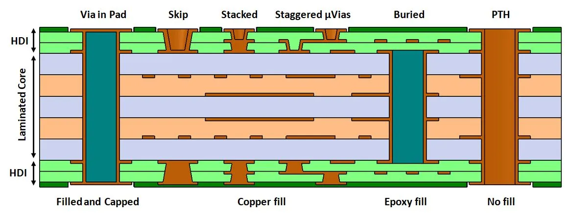
Layer Stacking and Routing
In HDI PCB design, microvias are often used in stacked or staggered configurations. Stacked microvias, where multiple microvias are aligned vertically across layers, offer the highest density but are more expensive to produce. Staggered microvias, offset between layers, are more cost-effective but require additional space. Choose the configuration based on your design’s complexity and cost targets.
Applications of Via-in-Pad Microvias in Modern Electronics
The use of via-in-pad microvias extends across various industries, driven by the demand for smaller, faster, and more efficient devices. Here are some common applications where this technology shines:
- Consumer Electronics: Smartphones and tablets rely on HDI PCBs with microvias to fit powerful processors and memory chips into tiny form factors.
- Automotive Systems: Advanced driver-assistance systems (ADAS) use fine-pitch BGAs with via-in-pad designs for reliable, high-speed data processing.
- Medical Devices: Wearable health monitors benefit from compact layouts enabled by microvias, ensuring portability without compromising functionality.
- Telecommunications: 5G infrastructure demands high-frequency performance, where microvia impedance control is critical for signal clarity.
Best Practices for Implementing Via-in-Pad Microvias
To ensure success with via-in-pad microvias in your next BGA design, follow these best practices:
- Collaborate Early with Fabricators: Discuss microvia capabilities and VIPPO requirements with your manufacturing partner to avoid design mismatches.
- Optimize Pad and Via Sizes: Use pad diameters at least 150 micrometers larger than the via to ensure reliable drilling and plating.
- Test for Reliability: Conduct thermal cycling and signal integrity tests on prototypes to validate microvia performance under real-world conditions.
- Focus on HDI Design Rules: Adhere to minimum trace widths (often 3-4 mils) and spacing rules for HDI layers to prevent manufacturing defects.
Conclusion: Unlocking the Potential of Via-in-Pad Microvias
Via-in-pad microvias, especially with VIPPO technology, are revolutionizing the way engineers approach BGA breakout and HDI PCB design. By enabling higher density, better signal integrity, and improved thermal management, these tiny structures pack a powerful punch for modern electronics. Whether you're tackling microvia impedance control or optimizing routing for fine-pitch BGAs, mastering this technology can elevate your designs to new heights.


