ALLPCB


If you're looking to ensure the quality of your printed circuit boards (PCBs) or troubleshoot internal issues, PCB microsectioning analysis is a powerful tool. This process, also known as PCB cross-section analysis, helps reveal hidden defects and verify manufacturing quality by examining the internal structure of a board. In this comprehensive guide, we'll explore the essentials of PCB microsection analysis, including its cost, the step-by-step procedure for cross-section analysis, and techniques for internal defect analysis. Whether you're an engineer, designer, or manufacturer, you'll find actionable insights to enhance your PCB production process.
What Is PCB Microsectioning Analysis?
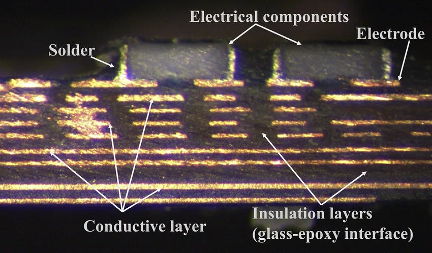
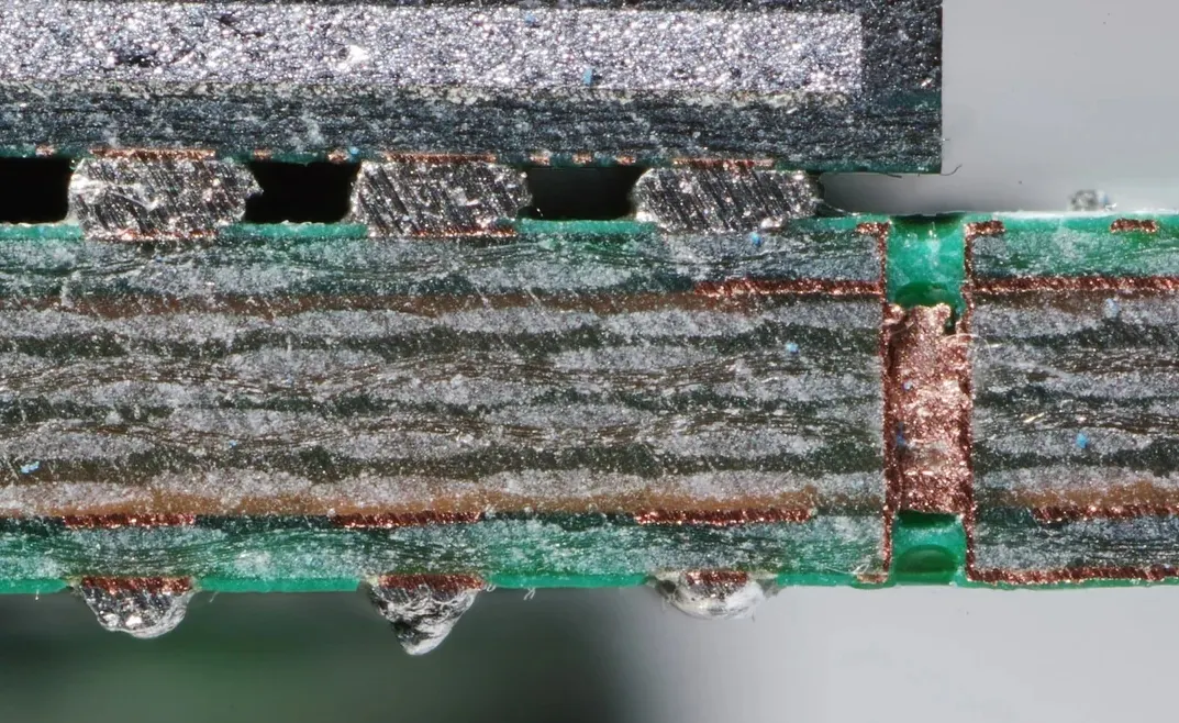
PCB microsectioning analysis is a detailed inspection method used to evaluate the internal structure of a printed circuit board. By cutting a small section of the PCB and examining it under a microscope, engineers can assess the quality of layers, plating, vias, and solder joints. This technique is critical for identifying defects that aren't visible on the surface, such as delamination, voids in plating, or misaligned layers. Often used in quality control and failure analysis, microsectioning provides a clear picture of a PCB's internal integrity.
Why Is PCB Microsectioning Analysis Important?
The reliability of electronic devices depends heavily on the quality of their PCBs. Even minor internal defects can lead to performance issues, such as signal loss or complete board failure. Microsectioning analysis helps in several key areas:
- Quality Assurance: Ensures that the PCB meets design specifications and industry standards like IPC-6012.
- Failure Analysis: Identifies the root cause of board failures by revealing hidden issues like cracks or poor plating.
- Process Improvement: Provides feedback on manufacturing processes, helping to refine techniques and reduce defects.
For high-stakes applications like aerospace or medical devices, where failure is not an option, this analysis is often a mandatory step. By catching issues early, manufacturers can avoid costly recalls or field failures.
Understanding PCB Microsection Analysis Cost
The cost of PCB microsection analysis can vary widely depending on several factors, including the complexity of the board, the equipment used, and the level of expertise required. On average, the cost for a basic microsection analysis can range from $100 to $500 per sample. For more advanced testing, such as those requiring high-resolution imaging or detailed reporting, costs can climb to $1,000 or more per board.
Here are the main factors that influence PCB microsection analysis cost:
- Sample Preparation: Cutting, mounting, and polishing the PCB sample requires specialized tools and skilled technicians, contributing to the overall cost.
- Equipment: High-end microscopes and imaging systems, such as scanning electron microscopes (SEM), can increase the price due to their precision and capabilities.
- Analysis Depth: A simple visual inspection is less expensive than a detailed report that includes measurements of copper thickness or via integrity.
- Volume: Testing multiple boards often reduces the per-sample cost due to economies of scale.
For small-scale projects or startups, these costs might seem high. However, investing in microsection analysis can save money in the long run by preventing defective boards from reaching the market. If budget is a concern, consider prioritizing critical boards or batches for testing rather than analyzing every single unit.
PCB Cross Section Analysis Procedure: Step by Step
The PCB cross-section analysis procedure is a meticulous process that requires precision and attention to detail. Below is a detailed breakdown of the steps involved in preparing and analyzing a PCB microsection:
Step 1: Sample Selection
Choose a representative sample from the batch of PCBs. This could be a board suspected of having defects or a random selection for quality control. The sample should reflect the overall production quality to ensure accurate results.
Step 2: Cutting the Sample
Using a precision cutting tool, such as a diamond saw, cut a small section from the PCB. The cut must be clean to avoid damaging the internal structures. Typically, the section is taken from an area of interest, like a via or a solder joint.
Step 3: Mounting the Sample
The cut section is embedded in a resin or epoxy material to hold it in place during further processing. This mounting step protects the delicate internal layers and ensures stability during polishing.
Step 4: Grinding and Polishing
The mounted sample is ground down to expose the internal structure and then polished to a smooth finish. This step is crucial for achieving a clear view under the microscope. Grinding too aggressively can introduce artifacts or damage, so it’s done gradually with finer abrasives.
Step 5: Microscopic Examination
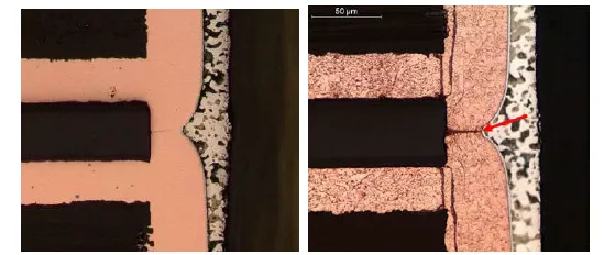
The polished sample is placed under a high-powered microscope for detailed inspection. Engineers look for issues like uneven copper plating (which should ideally be around 25-35 micrometers thick for standard boards), voids in vias, or delamination between layers. Measurements are often taken to ensure compliance with design specs.
Step 6: Documentation and Reporting
Findings are documented with high-resolution images and detailed notes. A comprehensive report might include measurements, such as the thickness of dielectric layers (often 100-200 micrometers in multilayer boards), and recommendations for addressing any defects found.
PCB Internal Defect Analysis: Techniques and Methods
Internal defects in PCBs can compromise performance, leading to issues like signal integrity loss (where impedance mismatches might deviate from the standard 50 ohms in high-speed designs) or outright failure. PCB internal defect analysis through microsectioning employs several techniques to identify and characterize these problems. Here are the most common methods used:
Visual Inspection Under Microscopy
The most straightforward method involves examining the cross-section under an optical microscope. This can reveal visible defects like cracks in the substrate, incomplete via filling, or separation between layers (delamination). For standard multilayer boards, layer alignment should be within a tolerance of ±50 micrometers to avoid signal issues.
Scanning Electron Microscopy (SEM)
For higher resolution, SEM is used to analyze finer details, such as micro-cracks or plating defects at the nanometer scale. This technique is particularly useful for identifying issues in high-density interconnect (HDI) boards where features are smaller than 100 micrometers.
Energy Dispersive X-Ray Spectroscopy (EDS)
EDS is often paired with SEM to analyze the material composition of specific areas. For example, it can detect contamination in solder joints or confirm the uniformity of copper plating. This is critical for ensuring that no foreign materials interfere with electrical conductivity.
Measurement of Key Parameters
During analysis, engineers measure critical dimensions like copper thickness, dielectric spacing, and via diameter. For instance, a typical via in a standard PCB might have a diameter of 0.3-0.8 mm, and any deviation could indicate a drilling or plating issue. These measurements help confirm whether the board meets design specifications.
Common internal defects identified through these methods include:
- Voids in Plating: Empty spaces in the copper plating of vias, which can disrupt electrical connectivity.
- Delamination: Separation of layers, often caused by poor adhesion or thermal stress, leading to mechanical weakness.
- Cracks: Fractures in the substrate or copper traces, which can interrupt signal paths.
- Misalignment: Layers not properly aligned, potentially causing short circuits or signal crosstalk in high-speed designs.
Benefits of Incorporating Microsectioning in Your Workflow
Adding PCB microsectioning analysis to your manufacturing or design process offers several advantages. First, it ensures that your boards meet stringent quality standards, reducing the risk of failures in the field. For high-speed applications, where signal integrity is critical, confirming impedance values (typically around 50 ohms for controlled impedance lines) through layer thickness measurements can make all the difference.
Second, it provides valuable feedback for process optimization. If recurring defects like uneven plating are identified, adjustments can be made to the fabrication process, such as tweaking the electroplating current density or bath chemistry. Over time, this leads to higher yields and lower production costs.
Finally, microsectioning builds trust with clients. Providing detailed analysis reports demonstrates a commitment to quality, which is especially important for industries like automotive or telecommunications, where reliability is non-negotiable.
Challenges and Limitations of PCB Microsectioning Analysis
While microsectioning is a powerful tool, it does come with some challenges. The process is destructive, meaning the tested board cannot be used afterward. For expensive or prototype boards, this can be a significant drawback. Additionally, the analysis requires skilled technicians and specialized equipment, which may not be available in-house for smaller companies.
Another limitation is that microsectioning only examines a small portion of the board. If defects are localized elsewhere, they might be missed. To mitigate this, multiple sections from different areas of the board can be analyzed, though this increases time and cost.
How to Choose a Reliable Service for PCB Microsection Analysis
If you lack the equipment or expertise to perform microsectioning in-house, partnering with a trusted testing service is a smart choice. Look for providers with experience in PCB analysis and a track record of delivering detailed, accurate reports. Ensure they follow industry standards like IPC-A-600 for acceptability of printed boards.
Additionally, check if the service offers customizable testing options. For instance, some projects may only need a basic visual inspection, while others require advanced SEM or EDS analysis. A good provider will tailor their services to your specific needs and budget.
Conclusion: Unlocking PCB Quality with Microsectioning Analysis
PCB microsectioning analysis is an invaluable technique for ensuring the quality and reliability of printed circuit boards. By understanding the PCB microsection analysis cost, mastering the PCB cross-section analysis procedure, and leveraging advanced methods for PCB internal defect analysis, you can significantly enhance your manufacturing process. Though it requires investment in terms of time and resources, the benefits of catching defects early, improving production techniques, and delivering high-quality boards far outweigh the costs.
Whether you're dealing with complex multilayer designs or high-speed applications, integrating microsectioning into your workflow provides the insights needed to build better PCBs. With the right approach and tools, you can uncover the hidden secrets of your boards and ensure they perform as intended in every application.