ALLPCB


In the fast-evolving world of electronics, High-Density Interconnect (HDI) PCBs are at the forefront of enabling compact, high-performance devices. However, with increased component density comes the challenge of managing heat effectively. If you're looking for solutions to HDI PCB thermal design, HDI PCB heat dissipation techniques, or the use of thermal vias in HDI PCBs, you're in the right place. This blog dives deep into proven strategies to keep your HDI PCBs cool and reliable under demanding conditions.
At ALLPCB, we understand the importance of thermal management in ensuring the longevity and performance of your designs. Below, we'll explore practical approaches, backed by technical insights, to help you tackle heat dissipation challenges in HDI PCBs. Let’s get started with a comprehensive guide to keeping your boards cool and efficient.
Why Thermal Management Matters for HDI PCBs
HDI PCBs are designed to pack more components into smaller spaces, using advanced techniques like microvias, blind vias, and buried vias. While this allows for sleeker, more powerful devices, it also means more heat is generated in a confined area. Without proper thermal management, excessive heat can lead to component failure, reduced efficiency, and even complete system breakdowns.
Studies show that for every 10°C rise in operating temperature, the lifespan of electronic components can be halved. In HDI designs, where components are closely spaced, heat dissipation becomes even more critical. Effective HDI PCB thermal design ensures that your board operates within safe temperature limits, maintaining performance and reliability.
Key Challenges in HDI PCB Thermal Design
Before diving into solutions, it’s important to understand the unique challenges of thermal management in HDI PCBs:
- High Component Density: More components in a smaller area generate concentrated heat, leaving little room for natural dissipation.
- Limited Space for Cooling Solutions: Traditional heat sinks or fans may not fit into compact HDI designs.
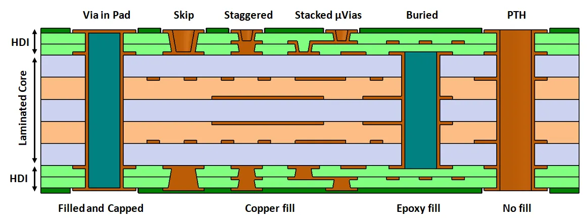
- Complex Layer Structures: Multiple layers with buried and blind vias can trap heat, making it harder to transfer to the surface.
- High Power Demands: Modern applications like AI servers or 5G devices often require higher power, leading to increased heat output.
Addressing these challenges requires a combination of innovative design techniques and material choices tailored to HDI PCB heat dissipation.
Effective HDI PCB Heat Dissipation Techniques
Let’s explore actionable strategies to manage heat in HDI PCBs. These techniques focus on design optimization, material selection, and advanced features like thermal vias.
1. Optimize Component Placement for Heat Distribution
Strategic placement of components is the first step in HDI PCB thermal design. Place high-power components, such as processors or power regulators, in areas with better airflow or closer to heat dissipation pathways. Avoid clustering heat-generating components together, as this creates hotspots that can damage the board.
For example, if a component generates 5W of heat, spacing it away from other heat sources and near a thermal via can reduce local temperature by up to 15-20%. Use simulation tools during the design phase to predict heat distribution and adjust layouts accordingly.
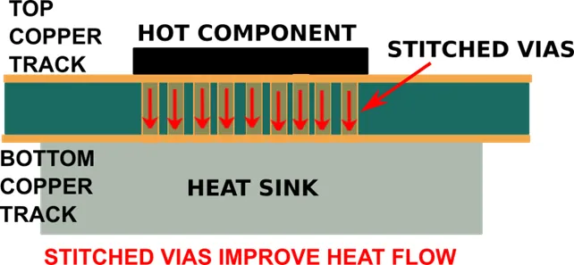
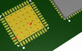
2. Use Thermal Vias in HDI PCB for Efficient Heat Transfer
Thermal vias are small, plated-through holes that act as conduits for heat, transferring it from hot components to other layers or external heat sinks. In HDI PCBs, where space is limited, thermal vias are especially effective. They can be placed directly under heat-generating components to create a direct path for heat to escape.
A common practice is to use an array of thermal vias with a diameter of 0.3-0.5mm, spaced 1-1.5mm apart, under high-power components. Research indicates that adding thermal vias can reduce junction temperatures by 10-25°C, depending on the via density and board thickness.
3. Select High-Thermal-Conductivity Materials
The choice of materials plays a significant role in HDI PCB heat dissipation techniques. Standard FR-4 materials have a thermal conductivity of about 0.3 W/m·K, which is often insufficient for high-power HDI designs. Instead, consider using advanced substrates like metal-core PCBs (MCPCBs) or materials with higher thermal conductivity, such as ceramic-based or high-Tg laminates, which can offer conductivity up to 1-3 W/m·K.
Additionally, copper thickness matters. Increasing the copper weight in critical layers (e.g., from 1oz to 2oz) can improve heat spreading by up to 30%, as copper has a thermal conductivity of approximately 400 W/m·K.
4. Incorporate Heat Sinks and Thermal Pads
While space constraints in HDI PCBs limit the use of large heat sinks, small, low-profile heat sinks or thermal pads can still be effective. Thermal pads, made of materials like silicone with thermal conductivity of 1-5 W/m·K, can be placed between components and the PCB to transfer heat away from critical areas.
For instance, attaching a small aluminum heat sink (thermal conductivity of 200 W/m·K) to a power IC can reduce its operating temperature by 10-15°C. Ensure proper mounting and contact to maximize heat transfer efficiency.
5. Leverage Multilayer Design for Heat Spreading
HDI PCBs often have multiple layers, which can be used to spread heat across the board. Dedicate internal copper layers as ground or power planes to act as heat spreaders. A solid copper plane can distribute heat more evenly, preventing localized hotspots.
For example, a 4-layer HDI PCB with a dedicated internal copper plane can reduce peak temperatures by 5-10°C compared to a design without such a plane. Ensure that thermal vias connect these planes to surface components for optimal results.
Advanced Thermal Management Techniques for HDI PCBs
Beyond the basics, there are advanced strategies that can further enhance thermal performance in HDI designs, especially for high-power applications.
1. Embedded Heat Pipes or Microchannels
For cutting-edge designs, embedding micro heat pipes or fluid channels within the PCB can provide exceptional heat dissipation. These systems use a small amount of liquid or vapor to transfer heat away from critical areas, achieving thermal conductivities equivalent to 1000-2000 W/m·K in some cases.
While this technique is more complex and costly, it’s ideal for applications like AI server motherboards, where heat loads can exceed 50W per component.
2. Active Cooling Solutions
In cases where passive cooling isn’t enough, active solutions like miniature fans or Peltier coolers can be integrated into the design. These are particularly useful for HDI PCBs in enclosed systems with no natural airflow. A small fan operating at 5V can reduce ambient temperatures around critical components by 20-30°C, though it adds to power consumption and design complexity.
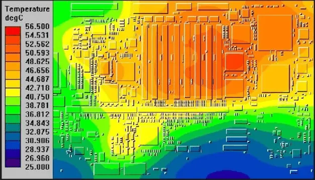
3. Thermal Simulation and Analysis
Before finalizing your HDI PCB thermal design, use thermal simulation software to model heat flow and identify potential issues. Tools can simulate temperature profiles under various operating conditions, helping you optimize via placement, material choices, and component layouts. For instance, simulations might reveal that increasing thermal via density under a 10W component reduces its temperature from 85°C to 65°C, well within safe limits.
Best Practices for Implementing Thermal Vias in HDI PCB
Since thermal vias are a cornerstone of HDI PCB heat dissipation techniques, let’s cover some best practices for their implementation:
- Placement: Position thermal vias directly beneath or adjacent to heat-generating components for maximum effect.
- Density: Use a grid pattern with 0.8-1.2mm spacing for high-power areas to balance heat transfer and structural integrity.
- Size: Opt for via diameters of 0.3-0.5mm to ensure manufacturability while maintaining effective heat conduction.
- Fill Material: Consider filling vias with conductive epoxy (thermal conductivity of ~10 W/m·K) to enhance heat transfer compared to unfilled vias.
- Connection: Connect thermal vias to large copper areas or heat sinks on the opposite side of the board for better dissipation.
Material and Manufacturing Considerations for Thermal Performance
The manufacturing process and material selection for HDI PCBs directly impact thermal management. Work closely with your PCB fabrication partner to ensure the following:
- High-Quality Copper Plating: Uniform copper plating in vias and layers ensures consistent heat conduction.
- Thermal Testing: Request thermal cycling tests during production to validate the board’s performance under heat stress.
- Layer Stackup Optimization: Collaborate on stackup design to balance signal integrity and thermal needs, especially in multilayer boards.
Choosing a reliable manufacturing partner can make a significant difference in achieving optimal thermal performance for your HDI designs.
Conclusion: Building Cooler, More Reliable HDI PCBs
Thermal management is a critical aspect of designing High-Density Interconnect PCBs, especially as devices become smaller and more powerful. By implementing effective HDI PCB thermal design strategies, such as optimizing component placement, using thermal vias in HDI PCBs, and selecting high-conductivity materials, you can significantly improve heat dissipation and extend the life of your electronics.
At ALLPCB, we’re committed to supporting your HDI PCB projects with advanced manufacturing capabilities and expert guidance. Whether you’re working on compact consumer gadgets or high-performance industrial systems, our team can help you achieve superior thermal performance. Start integrating these HDI PCB heat dissipation techniques into your next design, and experience the difference a well-cooled board can make.