ALLPCB


Security cameras have become an essential part of modern life, protecting homes, businesses, and public spaces. But have you ever wondered how the technology behind these devices, especially the printed circuit boards (PCBs), has evolved over time? In this blog, we’ll dive deep into the history of security camera PCBs, explore the evolution of CCTV electronics, highlight advancements in camera PCB technology, and discuss trends in security camera design. Whether you're an engineer, a tech enthusiast, or simply curious, this historical perspective will give you a clear understanding of how far we’ve come and where we’re headed.
Introduction: Why PCB Technology Matters in Security Cameras
Printed circuit boards are the backbone of any electronic device, including security cameras. They connect and support components like sensors, processors, and power systems, ensuring the camera functions reliably. Over the decades, the design and capabilities of these PCBs have transformed dramatically, enabling smaller, smarter, and more efficient security systems. From the bulky analog systems of the mid-20th century to today’s compact, AI-powered cameras, the evolution of CCTV electronics and PCB technology has played a pivotal role. Let’s take a journey through time to understand this transformation.
The Early Days: History of Security Camera PCBs (1940s-1960s)
The story of security cameras begins in the 1940s, when closed-circuit television (CCTV) systems were first developed for military purposes. In 1942, engineers in Germany used early CCTV to monitor rocket launches remotely. These systems relied on basic analog technology, with vacuum tubes and rudimentary wiring instead of modern PCBs. The concept of a printed circuit board as we know it today was still in its infancy, with early designs using flat metal strips on insulating boards to connect components, as pioneered by Albert Hanson in 1903.
By the late 1940s and early 1950s, commercial CCTV systems emerged for use in banks and government facilities. These setups used simple, hand-wired circuits or very basic PCBs with limited functionality. The boards were large, often made of phenolic paper or other early materials, and could only handle low-frequency signals. Power consumption was high, and reliability was a constant challenge due to heat dissipation issues and poor component integration.
During the 1960s, the introduction of transistor-based electronics marked a significant shift. Transistors replaced vacuum tubes, allowing for smaller and more efficient designs. PCBs for security cameras started to incorporate single-sided copper traces, enabling better organization of components. However, these early boards still lacked the complexity needed for advanced features like remote control or high-resolution imaging.
The Analog Era: Evolution of CCTV Electronics (1970s-1980s)
The 1970s and 1980s were a turning point for security camera technology as analog systems became more widespread. During this period, PCBs evolved from single-sided to double-sided designs, allowing for more components to be packed into a smaller space. This was crucial for integrating features like pan-tilt-zoom (PTZ) functionality and basic signal processing directly into the camera hardware.
Materials for PCBs also improved, with fiberglass replacing phenolic paper as the substrate of choice. Fiberglass offered better thermal stability and durability, which was essential for cameras installed in harsh outdoor environments. Signal integrity became a focus, with early attempts to manage impedance—often around 50 ohms for analog video signals—ensuring clearer image transmission over coaxial cables.
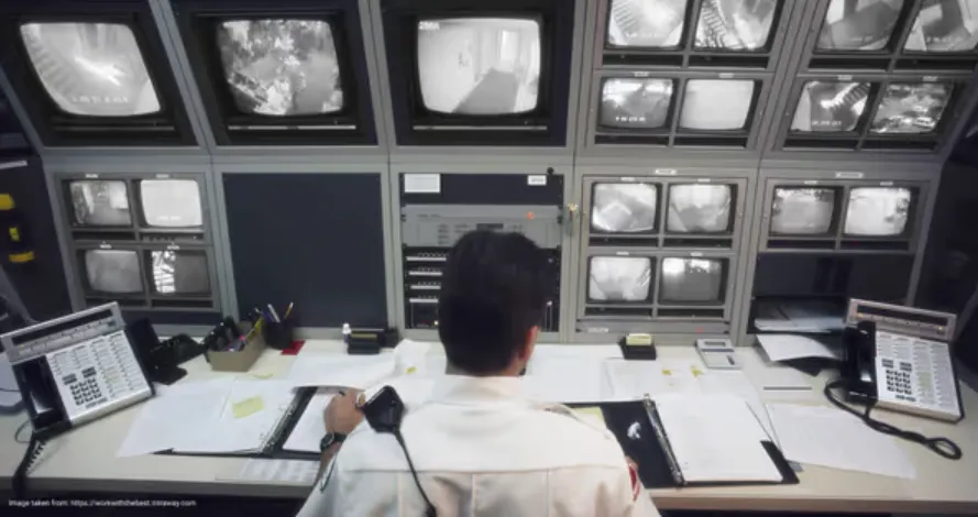
However, analog CCTV systems had limitations. Video quality was poor, often limited to resolutions below 480p, and frame rates were low, sometimes as little as 5-10 frames per second. PCBs during this era couldn’t support digital processing or compression, so recordings required bulky VHS tapes, and live monitoring was the primary use case. Despite these drawbacks, the evolution of CCTV electronics in this period laid the groundwork for future innovations.
Digital Revolution: Advancements in Camera PCB Technology (1990s-2000s)
The 1990s ushered in the digital age for security cameras, and with it came groundbreaking advancements in camera PCB technology. The shift from analog to digital required PCBs to handle higher data rates and more complex processing. Multi-layer PCBs became standard, often with 4 to 8 layers, allowing for separate power, ground, and signal planes. This design minimized electromagnetic interference (EMI) and supported the integration of digital signal processors (DSPs) and early microcontrollers.
One key development was the adoption of Charge-Coupled Device (CCD) sensors, followed by Complementary Metal-Oxide-Semiconductor (CMOS) sensors. These sensors converted light into digital signals, vastly improving image quality to resolutions of 720x480 pixels and beyond. PCBs had to accommodate higher-speed signals, often in the range of 10-100 MHz, to process and transmit this data. Impedance matching became critical, with controlled impedance traces (typically 50-75 ohms) ensuring minimal signal loss over longer distances.
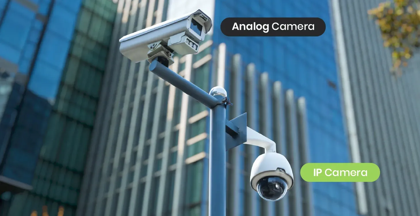
By the 2000s, the introduction of Internet Protocol (IP) cameras changed the game. These cameras used PCBs with embedded Ethernet controllers, enabling video streaming over networks. Power over Ethernet (PoE) technology also emerged, allowing a single cable to deliver both power and data, reducing wiring complexity. PCBs were now designed with tighter tolerances, often using high-frequency laminates to support data rates up to 100 Mbps for early IP cameras.
Modern Innovations: Trends in Security Camera Design (2010s-Present)
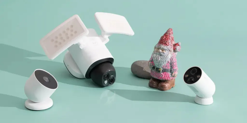
From the 2010s to today, security camera design and PCB technology have advanced at an incredible pace. Miniaturization has been a major trend, driven by the demand for discreet, compact cameras. Surface-mount technology (SMT) and microvia PCBs have made it possible to pack more functionality into smaller spaces. Modern security camera PCBs often feature 10 or more layers, with trace widths as small as 3 mils (0.003 inches) to accommodate high-density interconnects.
Another significant trend is the integration of artificial intelligence (AI) and machine learning directly into camera hardware. PCBs now include powerful System-on-Chip (SoC) solutions that handle real-time video analytics, such as facial recognition or motion detection. These chips require high-speed signal processing, often exceeding 1 GHz, and PCBs must support low-latency data transfer with minimal noise. Advanced materials like high-Tg FR-4 or even ceramic substrates are used to manage heat and maintain performance.
Wireless connectivity has also reshaped security camera design. PCBs are now designed with integrated Wi-Fi or 4G/5G modules, enabling remote access and cloud storage. This requires careful RF (radio frequency) design on the PCB, with impedance values precisely controlled at 50 ohms for antenna matching. Additionally, energy efficiency has become a priority, with power management circuits on PCBs reducing consumption to as low as 2-5 watts for small cameras.
Finally, environmental durability is a key focus. Modern PCBs for outdoor cameras use conformal coatings to protect against moisture and dust, and they’re designed to operate in temperature ranges from -40°C to 85°C. These advancements ensure reliability in extreme conditions, making security cameras more versatile than ever.
The Future: What’s Next for Security Camera PCB Technology?
Looking ahead, the evolution of security camera PCB technology shows no signs of slowing down. One exciting area is the integration of edge computing, where more processing happens directly on the camera. This will require even faster PCBs, potentially supporting data rates of 10 Gbps or higher, with advanced materials to handle thermal and electrical challenges.
Another trend is sustainability. As the electronics industry focuses on reducing waste, we may see more eco-friendly PCB materials, such as biodegradable substrates, and designs that prioritize repairability over replacement. Additionally, 5G connectivity will become standard, enabling ultra-high-definition video streaming at resolutions like 4K or 8K, which will demand PCBs with exceptional signal integrity.
Security itself is also a growing concern. Future PCBs may include hardware-based encryption modules to protect data from cyber threats, ensuring that video feeds remain secure. These innovations will continue to push the boundaries of what security cameras can do, making them smarter, smaller, and more reliable.
Conclusion: Reflecting on the Journey of Security Camera PCBs
The history of security camera PCBs is a fascinating tale of innovation and adaptation. From the simple, hand-wired circuits of the 1940s to the multi-layer, AI-enabled boards of today, the evolution of CCTV electronics and advancements in camera PCB technology have transformed how we monitor and protect our world. Trends in security camera design continue to push for smaller, smarter, and more sustainable solutions, and the future promises even more exciting developments.
At ALLPCB, we’re proud to be part of this journey, providing high-quality PCB solutions for cutting-edge security camera designs. Whether you’re developing the next big thing in surveillance or refining an existing product, understanding the historical perspective of PCB technology can inspire new ideas and approaches. Let’s keep building the future of security, one board at a time.