ALLPCB


If you're looking to streamline your PCB manufacturing process, understanding PCB tab routing and panelization techniques is essential. Tab routing is a widely used method in PCB panelization that involves creating small tabs to hold individual boards together within a panel during manufacturing, which are later removed during depanelization. This guide dives deep into PCB panelization methods, tab routing design rules, PCB assembly efficiency, depanelization techniques, and how these impact PCB manufacturing costs. Whether you're an engineer or a designer, you'll find actionable insights to optimize your production process for cost savings and efficiency.
What is PCB Panelization and Why Does It Matter?
PCB panelization is the process of grouping multiple printed circuit boards (PCBs) onto a single larger panel for manufacturing. This technique allows for easier handling, reduced material waste, and improved efficiency during assembly. By arranging several smaller boards into one panel, manufacturers can process them simultaneously, saving time and lowering PCB manufacturing costs.
Panelization is especially critical for small or irregularly shaped boards that are difficult to handle individually. It ensures stability during automated assembly processes like pick-and-place operations and soldering. However, the method of panelization—such as tab routing or V-scoring—plays a significant role in determining the ease of depanelization and the overall quality of the final product.
Understanding Tab Routing in PCB Panelization
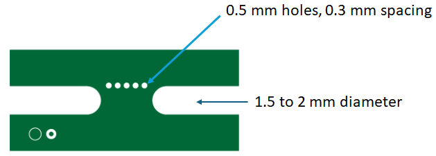
Tab routing is one of the most common PCB panelization methods. It involves creating small, breakable tabs (also called mouse bites) that connect individual PCBs to the panel frame or to each other. These tabs hold the boards securely during manufacturing but can be easily broken off during depanelization.
Unlike V-scoring, which uses a V-shaped groove to facilitate separation, tab routing relies on pre-drilled holes or perforations at the tab locations. This method is ideal for boards with irregular shapes or those requiring precise edges after separation, as it minimizes stress on the board compared to other depanelization techniques.
Advantages of Tab Routing
- Flexibility: Works well for non-rectangular or complex board shapes.
- Reduced Stress: Minimizes mechanical stress on the board during separation, preserving component integrity.
- Cost-Effective: Often more affordable than other methods for small to medium production runs, helping to control PCB manufacturing costs.
Challenges of Tab Routing
- Residual Tabs: After depanelization, small tab remnants may remain, requiring additional finishing.
- Space Requirements: Tabs take up space, potentially reducing the number of boards per panel.
Tab Routing Design Rules for Optimal Results
To achieve the best outcomes with tab routing, following specific design rules is crucial. These guidelines ensure that the tabs hold the boards securely during manufacturing while allowing for clean and easy separation during depanelization. Here are some key tab routing design rules to consider:
1. Tab Size and Spacing
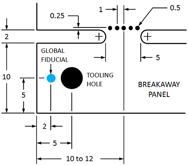
The size of the tabs should be large enough to provide stability but small enough to break easily. A common tab width is between 0.125 inches (3.175 mm) and 0.25 inches (6.35 mm), depending on the board thickness and material. Space tabs evenly along the board edges, typically placing 3-5 tabs per side for standard-sized boards (e.g., 2x2 inches or 50x50 mm).
2. Perforation Hole Size and Count
Mouse bite perforations usually consist of small holes drilled into the tab. A typical hole diameter is 0.02 inches (0.5 mm), with 5-7 holes per tab for a balance of strength and ease of breaking. Too few holes make the tab hard to break, while too many can weaken it excessively.
3. Tab Placement
Avoid placing tabs near sensitive components or traces to prevent damage during depanelization. Maintain a clearance of at least 0.1 inches (2.54 mm) between tabs and critical areas of the board. Additionally, position tabs on straight edges whenever possible to simplify the separation process.
4. Material Considerations
The PCB material impacts tab design. For standard FR-4 boards with a thickness of 0.062 inches (1.6 mm), standard tab sizes work well. Thicker or more brittle materials may require larger tabs or fewer perforations to avoid cracking during separation.
Enhancing PCB Assembly Efficiency with Proper Panelization
Effective panelization directly impacts PCB assembly efficiency. By optimizing the panel layout and tab routing design, manufacturers can streamline automated processes and reduce production time. Here are some strategies to boost efficiency:
Maximize Board Count per Panel
Arrange as many boards as possible on a single panel while maintaining adequate spacing for tabs and tooling holes. For instance, a panel size of 18x24 inches (457x610 mm) might accommodate 50 small boards of 2x2 inches each, significantly reducing handling time compared to processing them individually.
Use Tooling Holes and Fiducials
Include tooling holes (typically 0.125 inches or 3.175 mm in diameter) at the panel corners to ensure precise alignment during assembly. Add fiducial marks—small copper dots of 0.04 inches (1 mm) diameter—near the panel edges for automated vision systems to recognize board orientation, minimizing placement errors.
Balance Panel Strength and Depanelization Ease
Overly rigid panels can slow down assembly, while overly fragile ones risk breaking during handling. Tab routing strikes a balance by providing sufficient support without complicating the depanelization process, contributing to overall PCB assembly efficiency.
Depanelization Techniques for Tab-Routed PCBs
Depanelization is the process of separating individual PCBs from the panel after assembly. For tab-routed panels, several depanelization techniques can be used, each with its pros and cons. Choosing the right method depends on production volume, board material, and cost constraints.
1. Manual Breakaway
For low-volume production or prototyping, manually breaking the tabs by hand or with simple tools like pliers is common. This method is cost-effective but can be inconsistent, potentially leaving rough edges or causing stress to components near the tabs.
2. Punch and Die
A punch-and-die setup uses a custom tool to shear the tabs in a single motion. This method is faster and more precise than manual breakaway, suitable for medium-volume runs. However, it requires investment in tooling, which may increase PCB manufacturing costs for smaller projects.
3. Router Depanelization
For high-volume production or boards with complex shapes, a CNC router can cut through the tabs with high precision. This method leaves clean edges but is slower and more expensive due to the equipment and setup time involved.
4. Laser Depanelization
Laser cutting offers the highest precision and is ideal for delicate or thin boards (e.g., 0.031 inches or 0.8 mm thick). It eliminates mechanical stress but comes with a high cost, often reserved for specialized applications.
How Tab Routing Impacts PCB Manufacturing Costs
Tab routing plays a significant role in controlling PCB manufacturing costs. While it is generally a cost-effective panelization method, certain design choices and depanelization techniques can influence the overall expense. Here's how:
Material Utilization
Tab routing requires additional space for tabs and panel borders, which can reduce the number of boards per panel. For example, a panel that could fit 60 boards without tabs might only accommodate 50 with tab routing, increasing material costs per board by approximately 20%.
Depanelization Costs
Manual depanelization is the cheapest option, often costing less than $0.10 per board for small runs. In contrast, laser depanelization can cost $0.50 or more per board due to equipment and setup expenses, significantly impacting PCB manufacturing costs for larger volumes.
Finishing Requirements
After depanelization, tab remnants may require sanding or other finishing processes to achieve smooth edges. This additional labor can add $0.05 to $0.15 per board, depending on the level of precision needed.
By carefully designing tab placement and choosing an appropriate depanelization method, manufacturers can minimize these costs while maintaining quality and efficiency.
Best Practices for Combining Tab Routing with Other Panelization Methods
In some cases, combining tab routing with other PCB panelization methods like V-scoring can optimize efficiency and cost. For example, use V-scoring for straight edges to save space and reduce material waste, while applying tab routing for curved or irregular edges to ensure clean separation without stress.
When mixing methods, maintain consistent spacing between boards—typically 0.1 to 0.2 inches (2.54 to 5.08 mm)—to avoid alignment issues during assembly. Also, clearly document the panelization approach in your design files to prevent manufacturing errors.
Tips for Optimizing Your PCB Panelization Process
To wrap up, here are some practical tips to enhance your PCB panelization process using tab routing:
- Collaborate with Your Manufacturer: Share your design early to get feedback on panelization and tab routing options that suit their equipment and processes.
- Test Depanelization Early: Prototype your panel design to identify potential issues with tab strength or separation stress before full production.
- Standardize Panel Sizes: Stick to common panel dimensions like 9x12 inches (228x304 mm) or 18x24 inches (457x610 mm) to avoid custom tooling costs.
- Minimize Edge Components: Keep components at least 0.2 inches (5 mm) away from board edges to reduce the risk of damage during depanelization.
Conclusion
Mastering PCB tab routing and panelization techniques is a game-changer for achieving optimal efficiency in PCB manufacturing. By understanding tab routing design rules, prioritizing PCB assembly efficiency, selecting the right depanelization techniques, and managing PCB manufacturing costs, you can significantly improve your production outcomes. Whether you're working on a small prototype or a high-volume run, thoughtful panelization design ensures smoother processes, lower expenses, and high-quality results.
With the actionable insights provided in this guide, you're well-equipped to tackle the challenges of PCB panelization. Focus on balancing design flexibility with manufacturing constraints, and you'll see the benefits in both time and cost savings.