 ALLPCB


In the world of PCB design, dielectric thickness plays a critical role in ensuring signal integrity, especially for high-speed applications. Whether you're working on a simple circuit or a complex high-frequency board, understanding PCB dielectric thickness for signal integrity can make or break your design. So, what is dielectric thickness, and why does it matter? Simply put, dielectric thickness refers to the distance between conductive layers in a PCB, filled by an insulating material (dielectric) like FR-4. This thickness directly impacts impedance control, signal speed, and overall performance.
In this comprehensive guide, we'll dive deep into the importance of dielectric thickness impedance control, explore standard FR-4 dielectric thickness values, discuss considerations for high-speed PCB dielectric designs, and walk you through dielectric thickness calculation methods. By the end, you'll have actionable insights to optimize your PCB designs for better signal integrity.
What Is Dielectric Thickness in PCB Design?
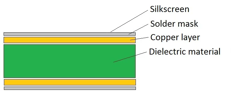
Dielectric thickness in a PCB refers to the measurement of the insulating material between two conductive layers, such as copper traces or planes. This insulating layer, often made of materials like FR-4, prevents electrical shorting while influencing how signals travel through the board. The dielectric material's properties, including its thickness and dielectric constant (Dk), affect the board's electrical performance.
For instance, in a typical four-layer PCB, dielectric layers separate the top layer from an internal ground plane, the ground plane from a power plane, and so on. The thickness of these layers isn't just about physical spacing; it determines critical factors like impedance and signal propagation delay. A thinner dielectric can reduce signal delay but may increase crosstalk, while a thicker dielectric might lower capacitance but slow down signals.
Why Dielectric Thickness Matters for Signal Integrity
Signal integrity refers to the quality of an electrical signal as it travels through a PCB. Issues like signal distortion, crosstalk, and timing errors can arise if the dielectric thickness isn't optimized. Here's why PCB dielectric thickness for signal integrity is so crucial:
- Impedance Control: Dielectric thickness directly affects the characteristic impedance of transmission lines. For high-speed signals, maintaining a specific impedance (like 50 ohms for many RF applications) is vital to prevent signal reflections.
- Signal Speed: The dielectric constant and thickness influence the speed at which signals propagate. A thinner dielectric with a lower Dk allows faster signal travel, which is critical for high-frequency designs.
- Crosstalk and Noise: If dielectric layers are too thin, signals on adjacent traces can interfere with each other, causing crosstalk. Proper thickness helps maintain isolation between signals.
Understanding and controlling dielectric thickness ensures that your PCB performs reliably, especially in demanding applications like telecommunications or automotive electronics.
Dielectric Thickness and Impedance Control: A Deep Dive
One of the most important aspects of dielectric thickness is its role in dielectric thickness impedance control. Impedance control ensures that the electrical characteristics of a trace match the requirements of the circuit, minimizing signal reflections and losses.
The characteristic impedance of a trace depends on several factors, including:
- Dielectric thickness (distance between the trace and the reference plane)
- Dielectric constant (Dk) of the material
- Trace width and thickness
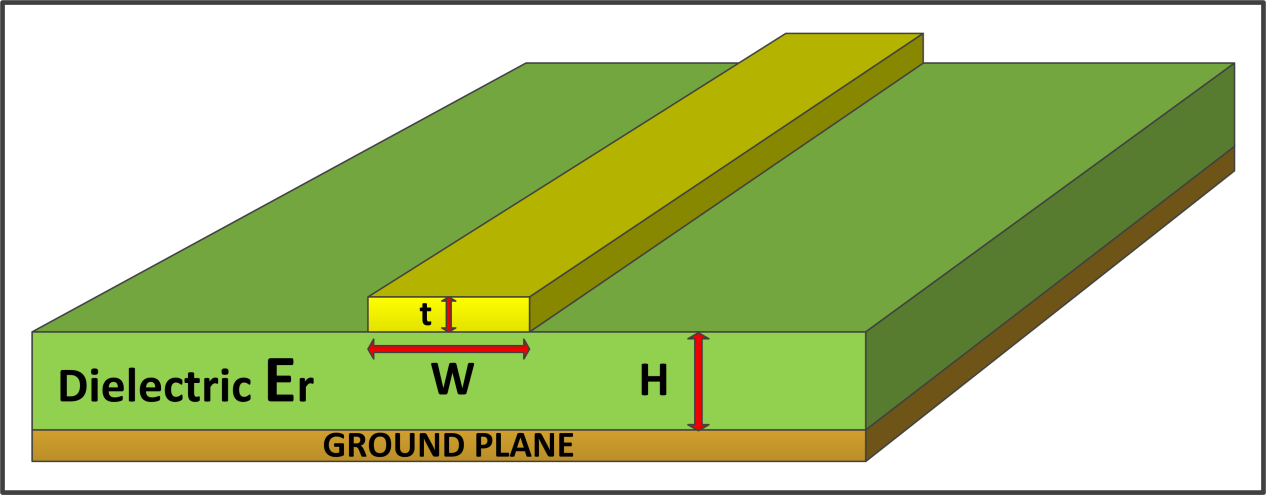
For example, in a microstrip configuration (a trace on the surface with a ground plane below), reducing the dielectric thickness increases capacitance, lowering the impedance. A common target impedance for high-speed digital signals is 50 ohms. If the dielectric thickness is 5 mils (0.005 inches) with a Dk of 4.2 (typical for FR-4), you might need a trace width of around 9 mils to achieve 50 ohms, depending on other stack-up factors. However, if the thickness increases to 10 mils, the trace width must be adjusted to maintain the same impedance.
Designers often use impedance calculators or simulation software to determine the right dielectric thickness and trace dimensions. Without precise control, mismatched impedance can cause signal reflections, leading to data errors in high-speed circuits.
Understanding FR-4 Dielectric Thickness: Industry Standards
FR-4 is the most widely used dielectric material in PCB manufacturing due to its cost-effectiveness and reliable performance. When discussing FR-4 dielectric thickness, it's important to know the standard values and how they apply to different designs.
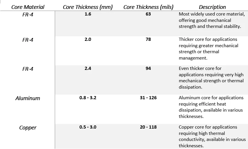
FR-4 boards typically come in standard overall thicknesses like 0.062 inches (1.6 mm), 0.031 inches (0.8 mm), and 0.093 inches (2.4 mm). However, the dielectric thickness between layers in a multilayer PCB is much thinner. Common dielectric thicknesses for FR-4 cores and prepregs (used in stack-ups) range from 3 mils (0.003 inches) to 20 mils (0.020 inches), depending on the layer count and design needs.
For a four-layer board, a typical stack-up might include:
- Top layer to ground plane: 5 mils dielectric
- Ground plane to power plane: 40 mils dielectric
- Power plane to bottom layer: 5 mils dielectric
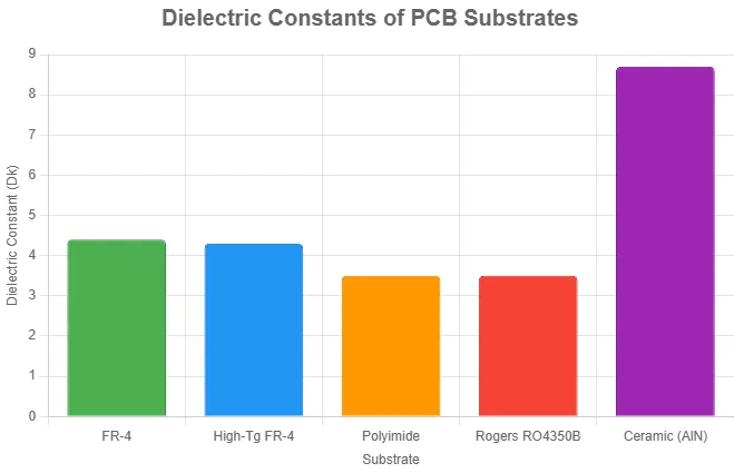
FR-4 has a dielectric constant (Dk) of around 4.2 to 4.5 at 1 MHz, though this value can vary with frequency and manufacturer. This Dk, combined with the dielectric thickness, affects signal speed and impedance. For standard designs, FR-4 is sufficient, but for very high frequencies (above 5 GHz), materials with lower Dk might be necessary.
High-Speed PCB Dielectric Considerations
In high-speed PCB dielectric designs, where signals operate at frequencies above 1 GHz or data rates exceed 5 Gbps, dielectric thickness becomes even more critical. High-speed signals are prone to losses, delays, and interference, so every aspect of the PCB stack-up must be carefully planned.
Key considerations for high-speed designs include:
- Thinner Dielectrics: Thinner dielectric layers reduce signal propagation delay and allow tighter impedance control. However, they can increase manufacturing costs and risk of crosstalk.
- Low Dk Materials: While FR-4 works for many applications, high-speed designs often use advanced laminates with Dk values below 3.5 to minimize signal loss.
- Uniform Thickness: Variations in dielectric thickness across the board can cause impedance mismatches, leading to signal integrity issues. Tight manufacturing tolerances are essential.
For instance, in a 10 Gbps design, a dielectric thickness variation of just 1 mil can cause a noticeable shift in impedance, potentially leading to bit errors. Designers must work closely with manufacturers to ensure consistent dielectric layers, especially in critical areas of the board.
How to Perform Dielectric Thickness Calculation
Calculating the right dielectric thickness for your PCB is a key step in achieving optimal performance. While dielectric thickness calculation can be complex, it generally involves determining the thickness needed to meet a specific impedance or signal speed requirement.
Here's a simplified process for calculating dielectric thickness for a microstrip trace targeting a specific impedance:
- Determine Target Impedance: Identify the required impedance (e.g., 50 ohms for many high-speed signals).
- Know the Dielectric Constant: Use the Dk of your material (e.g., 4.2 for FR-4).
- Estimate Trace Width: Start with an approximate trace width based on standard guidelines or past designs.
- Use an Impedance Formula or Tool: Apply a microstrip impedance formula or use a calculator tool. A common approximation for microstrip impedance is based on the formula: Z = (87 / √(Dk + 1.41)) * ln(5.98 * H / (0.8 * W + T)), where H is dielectric thickness, W is trace width, and T is trace thickness (all in mils).
- Adjust Thickness: Solve for H (dielectric thickness) by inputting the desired Z and other known values. Iterate if necessary to balance with manufacturing constraints.
For example, to achieve 50 ohms with a trace width of 10 mils and trace thickness of 1.4 mils on FR-4 (Dk = 4.2), you might calculate a dielectric thickness of around 6 mils. However, real-world designs often require simulation tools for accuracy, as factors like frequency-dependent Dk and manufacturing tolerances come into play.
Always collaborate with your PCB manufacturer to confirm achievable dielectric thicknesses, as standard prepreg and core materials may limit your options. Additionally, consider stack-up symmetry to avoid warping during production.
Practical Tips for Optimizing Dielectric Thickness in Your Designs
Now that we've covered the fundamentals, here are some practical tips to help you optimize dielectric thickness in your PCB designs:
- Start with Standard Stack-Ups: Use manufacturer-recommended stack-ups for common layer counts to simplify design and reduce costs. Adjust dielectric thickness only if necessary for impedance or signal speed.
- Simulate Before Building: Use PCB design software to simulate signal behavior with different dielectric thicknesses. This helps identify potential issues before manufacturing.
- Consider Manufacturing Tolerances: Dielectric thickness can vary by ±10% or more due to manufacturing processes. Design with some margin to account for these variations.
- Balance Cost and Performance: Thinner dielectrics and advanced materials improve performance but increase costs. Evaluate whether the benefits justify the added expense for your application.
- Test Prototypes: For critical designs, build and test prototypes to measure actual impedance and signal integrity. Adjust dielectric thickness in subsequent revisions if needed.
Common Mistakes to Avoid with Dielectric Thickness
Even experienced designers can make mistakes when dealing with dielectric thickness. Here are some pitfalls to watch out for:
- Ignoring Frequency Effects: The dielectric constant of materials like FR-4 changes with frequency. Don't assume a static Dk value for high-speed designs.
- Overlooking Stack-Up Symmetry: Uneven dielectric thicknesses can cause board warping during manufacturing. Ensure a balanced stack-up.
- Neglecting Crosstalk: Very thin dielectrics can lead to signal interference between layers. Maintain adequate spacing for your signal frequencies.
- Assuming Uniform Thickness: Resin flow during lamination can cause slight variations in dielectric thickness. Work with your manufacturer to minimize these inconsistencies.
Conclusion: Mastering Dielectric Thickness for Superior PCB Performance
Dielectric thickness is a foundational element of PCB design that directly impacts signal integrity, impedance control, and overall performance. By understanding concepts like PCB dielectric thickness for signal integrity, mastering dielectric thickness impedance control, and applying the right FR-4 dielectric thickness or high-speed PCB dielectric strategies, you can create reliable and efficient designs. Additionally, learning dielectric thickness calculation methods empowers you to fine-tune your stack-ups for specific requirements.
Whether you're designing a simple two-layer board or a complex high-speed system, paying attention to dielectric thickness ensures your signals travel cleanly and without interference. Use the tips and insights from this guide to elevate your PCB designs, and always collaborate with your manufacturing partner to achieve the best results.
With the right approach, you can master dielectric thickness and build PCBs that meet the demands of modern electronics. Keep experimenting, testing, and refining your designs to stay ahead in this ever-evolving field.


