 ALLPCB


When designing a printed circuit board (PCB), every detail matters, especially when it comes to V-scoring and component placement. V-scoring, a method used to create grooves on a PCB panel for easy separation after assembly, directly impacts how and where components are placed. For engineers searching for guidance on "V-scoring component placement," "V-scoring keepout zones," "V-scoring design rules," or "component distance from V-score," the key takeaway is this: V-scoring requires careful planning to avoid mechanical stress, ensure board integrity, and maintain functionality during and after separation. In this blog, we’ll dive deep into how V-scoring affects PCB design, offering practical tips and rules to help you create reliable and efficient layouts.
What is V-Scoring and Why Does It Matter in PCB Design?
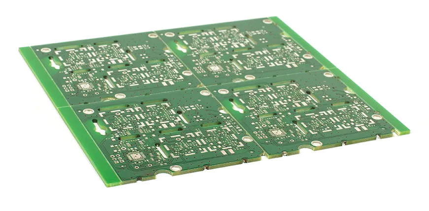
V-scoring, also known as V-grooving or V-cutting, is a technique used in PCB manufacturing to create predefined separation lines on a panel of multiple boards. These "V"-shaped grooves are cut into both the top and bottom surfaces of the board, leaving a thin strip of material in the middle. This makes it easy to snap the individual boards apart after assembly, much like breaking a chocolate bar along its lines.
The primary purpose of V-scoring is to streamline the manufacturing process. By panelizing multiple PCBs into a single unit, assembly becomes more efficient, especially for automated surface-mount technology (SMT) processes. However, while V-scoring offers convenience, it introduces mechanical stress points that can affect the board’s structural integrity and the components placed near these grooves. This is why understanding its impact on component placement is critical for any PCB designer aiming for reliability and performance.
How V-Scoring Affects Component Placement
The placement of components on a PCB is a delicate balancing act, and V-scoring adds an extra layer of complexity. When grooves are cut into the board, they weaken the material along those lines, making the area prone to stress, cracks, or even unintended breakage during handling or separation. Here’s how V-scoring specifically impacts where and how you place components:
- Mechanical Stress: The process of snapping the board apart after PCB assembly can create vibrations or stress that may damage delicate components or solder joints near the V-score line.
- Board Warpage: Uneven stress distribution caused by V-scoring can lead to board warpage, which might misalign components or affect electrical connections.
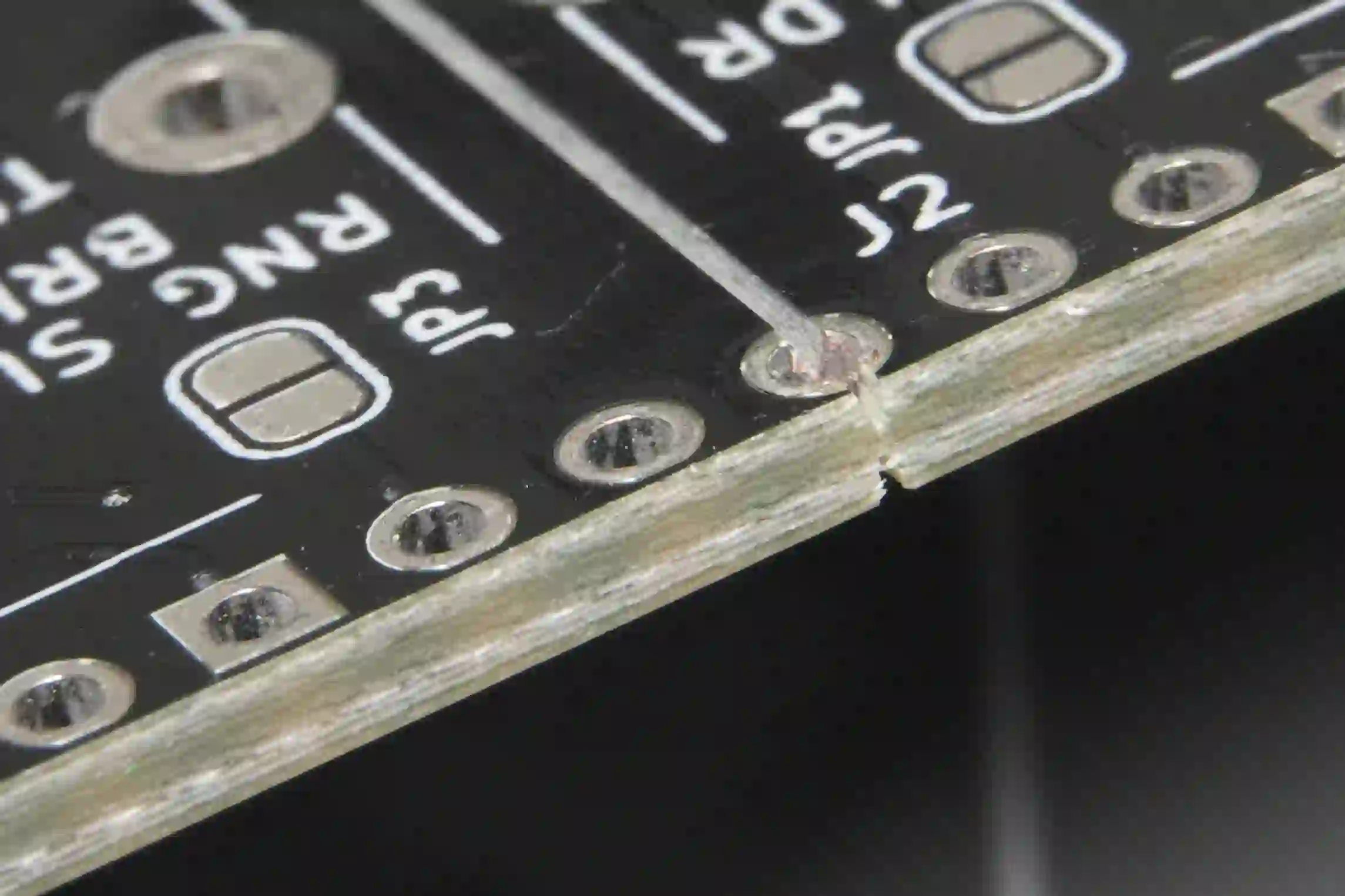
- Trace Integrity: Running traces too close to a V-score risks fracturing them during separation, leading to open circuits or unreliable performance.
For these reasons, designers must follow specific guidelines when placing components near V-scoring lines. Ignoring these considerations can result in costly rework or product failures down the line.
Key V-Scoring Design Rules for Component Placement
To mitigate the risks associated with V-scoring, there are established design rules that focus on component placement and board layout. These rules help ensure that your PCB remains functional and durable throughout its lifecycle. Below are some essential "V-scoring design rules" to keep in mind:
1. Maintain Adequate Component Distance from V-Score Lines
One of the most critical rules is maintaining a safe distance between components and the V-score line. As a general guideline, components should be placed at least 5 mm (0.2 inches) away from the scored edge. For larger or heavier components, such as connectors or electrolytic capacitors, this distance should increase to 8-10 mm (0.3-0.4 inches) to account for the greater risk of mechanical shock during separation.
This "component distance from V-score" rule helps protect against stress-induced damage. For example, a surface-mount resistor placed too close to the V-score might experience cracked solder joints when the board is snapped apart, leading to intermittent connections or complete failure.
2. Define V-Scoring Keepout Zones
A keepout zone is an area on the PCB where no components, traces, or vias are allowed. When dealing with V-scoring, defining "V-scoring keepout zones" is a must. Typically, this zone extends 3-5 mm (0.12-0.2 inches) on either side of the V-score line, depending on the board thickness and material. For standard FR-4 boards with a thickness of 1.6 mm, a 3 mm keepout zone is often sufficient. However, for thinner boards (e.g., 0.8 mm), a wider zone of 5 mm is recommended due to their increased fragility.
Keepout zones prevent components and traces from being damaged during the scoring or separation process. They also reduce the risk of microcracks forming in the PCB material, which could propagate over time and compromise the board’s reliability.
3. Avoid Placing High-Stress Components Near V-Scores
Certain components, such as large through-hole components, heavy connectors, or heat sinks, exert more mechanical stress on the PCB due to their size and weight. Placing these near a V-score line increases the likelihood of board damage during handling or separation. As a rule, position high-stress components at least 10 mm (0.4 inches) away from the scored edge, and consider reinforcing the board with additional mounting points if needed.
For instance, a power connector weighing 10 grams placed just 2 mm from a V-score line might cause the board to crack prematurely during assembly. Moving it farther away or adding a support bracket can prevent such issues.
4. Protect Traces and Vias Near V-Scoring Lines
Electrical traces and vias are just as vulnerable to damage as components. Running traces parallel to a V-score line within 3 mm (0.12 inches) risks fracturing them during separation, which can disrupt critical signals. If traces must cross a V-score area, ensure they are routed perpendicular to the line to minimize the length exposed to potential stress. Additionally, avoid placing vias within the keepout zone, as they can weaken the board further and act as stress concentration points.
Additional Design Considerations for V-Scoring and Component Placement
Beyond the core rules, there are other factors to consider when integrating V-scoring into your PCB design. These considerations ensure that your board not only functions well but also withstands the rigors of manufacturing and assembly.
Board Thickness and Material
The thickness and material of your PCB play a significant role in how V-scoring affects component placement. Thicker boards (e.g., 2.0 mm or more) are generally more robust and can tolerate components placed closer to the V-score line, with a minimum distance of around 3 mm. However, thinner boards (e.g., 0.6-0.8 mm) are more prone to bending and cracking, so a larger keepout zone of 5-7 mm is advisable.
Material choice also matters. Standard FR-4 is relatively durable, but flexible or high-frequency materials like polyimide or Rogers may require wider keepout zones due to their different mechanical properties. Always consult your manufacturing partner for specific recommendations based on the material you’re using.
Panel Layout and V-Score Orientation
The way you arrange individual boards within a panel affects V-scoring and component placement. For example, orienting V-score lines along the shorter edges of a rectangular board can reduce stress compared to scoring along the longer edges. Additionally, ensure that the panel layout allows for uniform scoring depth—typically 30-50% of the board thickness per side (e.g., 0.5 mm deep cuts on each side of a 1.6 mm board)—to avoid uneven stress distribution that could impact nearby components.
Stress Testing and Simulation
Before finalizing your design, consider using simulation tools to model the mechanical stress caused by V-scoring. Software can predict how snapping the board will affect components and traces, allowing you to adjust placement accordingly. For high-reliability applications, such as aerospace or medical devices, physical stress testing on a prototype panel is also recommended to validate your "V-scoring component placement" strategy.
Best Practices for Optimizing V-Scoring in PCB Design
To wrap up, let’s cover some best practices that tie together the concepts of V-scoring and component placement. These tips will help you create designs that are both manufacturable and reliable:
- Collaborate Early with Your Manufacturer: Different fabrication houses may have specific V-scoring capabilities or constraints. Share your design files early to ensure compliance with their processes, especially regarding groove depth and spacing.
- Use Design Software Features: Most PCB design tools allow you to define keepout zones and set rules for component placement near V-score lines. Leverage these features to automate compliance with design guidelines.
- Prioritize Component Grouping: Group similar components away from V-score lines to simplify assembly and reduce the risk of damage. For example, place all SMT components in a central cluster, leaving the edges free for scoring.
- Document V-Scoring Specifications: Clearly annotate V-score lines and keepout zones in your design files. Include notes on groove depth (e.g., 0.5 mm per side) and minimum distances to ensure the manufacturer follows your intent.
Conclusion: Balancing V-Scoring and Component Placement for Success
V-scoring is a powerful tool for efficient PCB manufacturing, but it comes with challenges that directly impact component placement. By adhering to key "V-scoring design rules," maintaining proper "component distance from V-score," and defining clear "V-scoring keepout zones," you can minimize risks and ensure your design performs as intended. Whether you’re working on a simple prototype or a complex multilayer board, thoughtful "V-scoring component placement" is essential for achieving reliability and manufacturability.
At ALLPCB, we’re committed to helping engineers navigate the intricacies of PCB design. By incorporating these guidelines into your workflow, you’ll be better equipped to create boards that stand up to the stresses of V-scoring while delivering top-notch performance. Keep these tips in mind for your next project, and you’ll see the difference in both quality and efficiency.


