ALLPCB


Rigid-Flex Stackup Considerations for Signal Integrity in Flexible Circuits
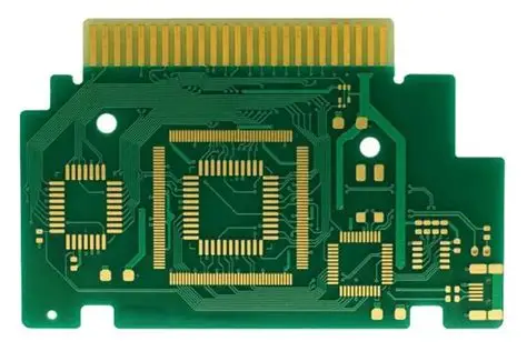
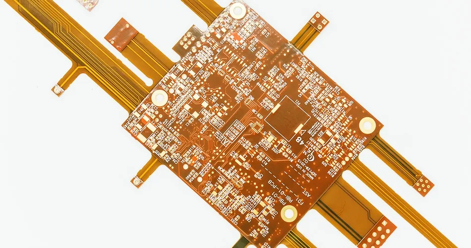
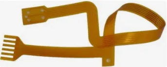
Rigid-flex printed circuit boards combine rigid sections for component mounting with flexible sections that enable bending and folding in compact assemblies. Engineers rely on these hybrid constructions in applications ranging from aerospace avionics to medical devices where space constraints and mechanical movement coexist. The stackup configuration directly influences electrical performance, particularly signal integrity across high-speed traces that traverse both rigid and flexible zones. Proper planning of layer arrangement, material selection, and transition management helps maintain consistent impedance and minimizes reflections or losses.
What Is Rigid-Flex PCB Stackup and Why It Matters
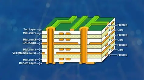
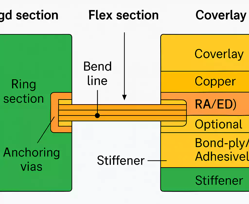
A rigid-flex PCB stackup defines the sequence and composition of conductive copper layers, dielectric materials, adhesives, and coverlays that form the board. Rigid portions typically incorporate glass-reinforced epoxy laminates similar to standard FR-4 constructions, while flexible sections use polyimide films with rolled annealed copper for repeated flexing. The transition zones between rigid and flexible areas require careful design to avoid abrupt changes in electrical characteristics.
Signal integrity in flex PCB designs depends on maintaining controlled impedance along the entire trace path. Variations in dielectric constant, trace geometry, or reference plane continuity at the rigid-to-flex interface can introduce discontinuities that degrade rise times or increase crosstalk. Industry standards such as IPC-2223 provide sectional design guidelines that address these stackup variables for flexible and rigid-flex circuits. Early attention to stackup symmetry and material properties supports reliable performance in both static and dynamic bending environments.
Technical Principles of Stackup Design for Signal Integrity
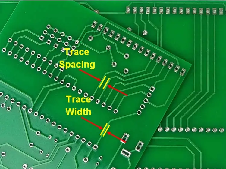
Impedance control in rigid-flex constructions begins with selecting dielectric thicknesses and copper weights that achieve target values, often 50 ohms single-ended or 100 ohms differential. In flexible sections the lower dielectric constant of polyimide compared with rigid laminates requires adjustments in trace width or spacing to compensate. Reference planes must remain continuous or properly stitched across transitions to provide stable return paths for high-frequency currents.
Dynamic bending introduces additional variables because flexing alters the physical spacing between conductors and changes local strain on copper traces. Traces routed parallel to the bend axis experience different stress than those perpendicular to it, potentially affecting characteristic impedance during operation. Rolled annealed copper foils are preferred in flex zones for their superior fatigue resistance, while electrodeposited copper suits rigid areas where mechanical demands differ.
Transition zones represent critical points where layer terminations, adhesive fillets, and coverlay overlaps can create localized impedance variations. Maintaining consistent copper distribution and avoiding abrupt changes in dielectric thickness helps preserve signal quality. Ground planes in flex regions often employ cross-hatching patterns to improve flexibility without excessively compromising shielding effectiveness or impedance stability.
Practical Solutions and Best Practices for Stackup Optimization
Designers achieve reliable impedance control rigid-flex performance by starting with a symmetrical stackup that balances copper distribution above and below the neutral axis in flex sections. This symmetry reduces warpage tendencies and supports consistent electrical behavior. Placing high-speed signals adjacent to solid reference planes in both rigid and flex areas minimizes loop inductance and stabilizes impedance.
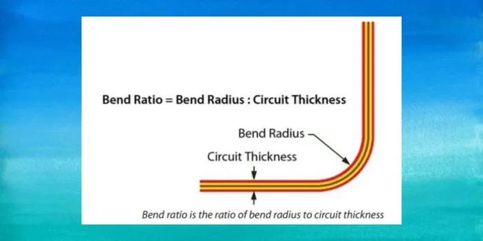
Trace routing guidelines recommend keeping critical signals away from bend radii where possible or orienting them to minimize strain. In dynamic applications, minimum bend radii follow recommendations in established design standards to limit mechanical stress on conductors. Via placement avoids flex zones entirely, with transitions handled through carefully designed pad or anchor features that maintain continuity.
Material choices influence both manufacturability and electrical outcomes. Low-loss polyimide variants help reduce insertion loss in high-speed flex circuits, while adhesive systems are selected for low dielectric loss and thermal stability. Collaboration between design and fabrication teams early in the process allows modeling of specific stackup configurations to verify impedance targets before committing to production.
Best Practices for Dynamic Bending Signal Integrity
For applications involving repeated flexing, stackup designs incorporate additional margins in dielectric thickness and copper ductility. Shielding layers or embedded ground planes in flex sections can suppress electromagnetic interference while preserving flexibility through patterned constructions. Testing protocols often include time-domain reflectometry measurements to confirm impedance consistency before and after bending cycles.
Engineers also consider thermal expansion mismatches between rigid and flex materials during stackup definition. Coefficient of thermal expansion alignment reduces stress concentrations that could indirectly affect long-term signal integrity through micro-cracking or delamination. IPC-6013 outlines qualification requirements that encompass both electrical and mechanical performance for flexible and rigid-flex boards.
Conclusion
Effective rigid-flex PCB stackup design integrates electrical, mechanical, and manufacturing considerations to preserve signal integrity throughout the product lifecycle. Attention to impedance continuity, reference plane integrity, and transition zone details enables high-speed performance in space-constrained, movable assemblies. Adherence to established industry standards such as IPC-2223 and IPC-6013 provides a framework for consistent, reliable outcomes across diverse applications.
FAQs
Q1: What factors most influence impedance control in rigid-flex PCB stackup designs?
A1: Dielectric material selection, trace geometry, reference plane continuity, and transition zone construction primarily determine impedance behavior. Adjustments in trace width compensate for differences in dielectric constant between rigid and flex sections. Consistent stackup symmetry further supports stable performance under bending conditions.
Q2: How does dynamic bending affect signal integrity in flexible circuit stackup designs?
A2: Repeated flexing can alter conductor spacing and introduce mechanical strain that shifts local impedance values. Proper material choices such as rolled annealed copper and adherence to minimum bend radius guidelines help maintain electrical consistency. Cross-hatched ground planes and optimized trace routing directions mitigate these effects.
Q3: Why is reference plane continuity important across rigid-flex transitions?
A3: Continuous or well-stitched reference planes ensure predictable return current paths and minimize impedance discontinuities that cause reflections. Disruptions at transition zones degrade signal quality, especially at higher frequencies. Stackup planning that preserves plane integrity supports overall signal integrity flex PCB performance.
Q4: What role do industry standards play in flexible circuit stackup design?
A4: Standards such as IPC-2223 guide layer arrangement, bend radius calculations, and material considerations for reliable flexible constructions. IPC-6013 establishes performance and qualification criteria that encompass both electrical and mechanical requirements for rigid-flex boards. Following these guidelines promotes designs that meet functional and durability expectations.