 ALLPCB


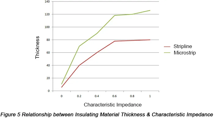
If you're wondering how prepreg thickness affects PCB impedance control, here's the quick answer: Prepreg thickness directly influences the dielectric spacing between conductive layers in a printed circuit board (PCB), which in turn impacts the characteristic impedance of transmission lines like microstrip and stripline. A thicker prepreg increases the distance between layers, lowering the impedance, while a thinner prepreg does the opposite. This relationship is critical for maintaining signal integrity in high-frequency circuits.
In this comprehensive guide, we'll explore the intricate connection between prepreg thickness and impedance control in PCBs. We'll break down key concepts like controlled impedance PCB design, microstrip impedance, and stripline impedance, offering practical insights for engineers and designers. Whether you're working on high-speed digital circuits or RF applications, understanding these factors can help you design more reliable and efficient boards.
What is Prepreg and Why Does It Matter in PCB Design?
Prepreg, short for "pre-impregnated," is a fiberglass material soaked with resin and used as an insulating layer between copper layers in a multilayer PCB. It acts as a dielectric medium, bonding the layers together during the lamination process while maintaining electrical isolation. The thickness of prepreg varies depending on the type and number of layers used, typically ranging from 0.002 inches (2 mils) to 0.010 inches (10 mils) or more.
In the context of PCB impedance control, prepreg thickness plays a pivotal role because it determines the spacing between conductive traces and ground planes. This spacing, along with the dielectric constant of the prepreg material (often around 3.5 to 4.5 for standard FR-4 materials), directly affects the characteristic impedance of the transmission lines on the board. For high-frequency signals, even a small variation in prepreg thickness can lead to impedance mismatches, causing signal reflections, crosstalk, or data loss.
Understanding PCB Impedance Control
Before diving deeper into prepreg thickness, let's clarify what PCB impedance control means. Impedance control refers to designing a PCB so that the characteristic impedance of its transmission lines matches the source and load impedances in a circuit. This is crucial for high-speed and high-frequency applications, where mismatched impedance can degrade signal integrity.
Characteristic impedance, often denoted as Z?, is typically measured in ohms (Ω). Common values for controlled impedance PCBs are 50Ω for single-ended lines and 100Ω for differential pairs. Achieving these values requires precise control over several factors, including trace width, trace thickness, dielectric material properties, and—most relevant to this discussion—prepreg thickness.
In a controlled impedance PCB, designers aim to minimize signal reflections and ensure efficient power transfer. This is especially important in applications like USB, HDMI, Ethernet, and RF circuits, where signal speeds can exceed 1 GHz. A deviation of just a few ohms from the target impedance can introduce noise or timing errors, leading to system failures.
How Prepreg Thickness Affects Microstrip Impedance
Microstrip is a type of transmission line commonly used on the outer layers of a PCB. It consists of a conductive trace on the surface of the board, separated from a ground plane by a dielectric layer, often made of prepreg or core material. The impedance of a microstrip line is influenced by the trace width, the dielectric constant of the material, and the distance between the trace and the ground plane (i.e., the prepreg thickness).
For a typical microstrip line on an FR-4 substrate with a dielectric constant of 4.2, increasing the prepreg thickness from 5 mils to 10 mils can reduce the characteristic impedance from approximately 50Ω to 45Ω, assuming a constant trace width of 6 mils. This happens because a thicker dielectric increases the distance between the trace and ground plane, reducing the capacitance per unit length and thus lowering the impedance.
Designers often use impedance calculators or simulation tools to predict these values and select the appropriate prepreg thickness during the stack-up design phase. Maintaining tight tolerances on prepreg thickness—typically within ±10%—is essential to ensure consistent microstrip impedance across the board.
The Role of Prepreg Thickness in Stripline Impedance
Unlike microstrip, stripline is a transmission line embedded between two ground planes within the internal layers of a PCB. It offers better electromagnetic interference (EMI) shielding due to its sandwiched structure but is more sensitive to variations in prepreg thickness. In a stripline configuration, the trace is surrounded by dielectric material on both sides, and the impedance depends on the trace width, dielectric constant, and the total thickness of the dielectric layers (often two layers of prepreg or a combination of prepreg and core).
For a stripline with a target impedance of 50Ω, using a dielectric constant of 4.0, a trace width of 5 mils, and a total dielectric thickness of 10 mils (5 mils per side), a 1-mil increase in prepreg thickness on each side could lower the impedance to around 48Ω. This change might seem small, but in high-frequency designs operating at 5 GHz or more, even a 2Ω deviation can cause significant signal distortion.
Stripline designs often require tighter control over prepreg thickness because variations affect both sides of the trace. Manufacturers must carefully select prepreg materials and stack-up configurations to meet the specified impedance targets.
Challenges in Maintaining Prepreg Thickness for Impedance Control
While prepreg thickness is a critical parameter for PCB impedance control, maintaining consistency during manufacturing can be challenging. Here are some common issues designers and fabricators face:
- Material Variability: Different batches of prepreg material may have slight variations in thickness or dielectric constant, even when sourced from the same supplier. For instance, a specified 5-mil prepreg might measure between 4.8 and 5.2 mils, impacting impedance calculations.
- Lamination Pressure and Temperature: During the lamination process, pressure and heat can compress prepreg layers, reducing their thickness by up to 10-15%. This compression must be accounted for in the initial design.
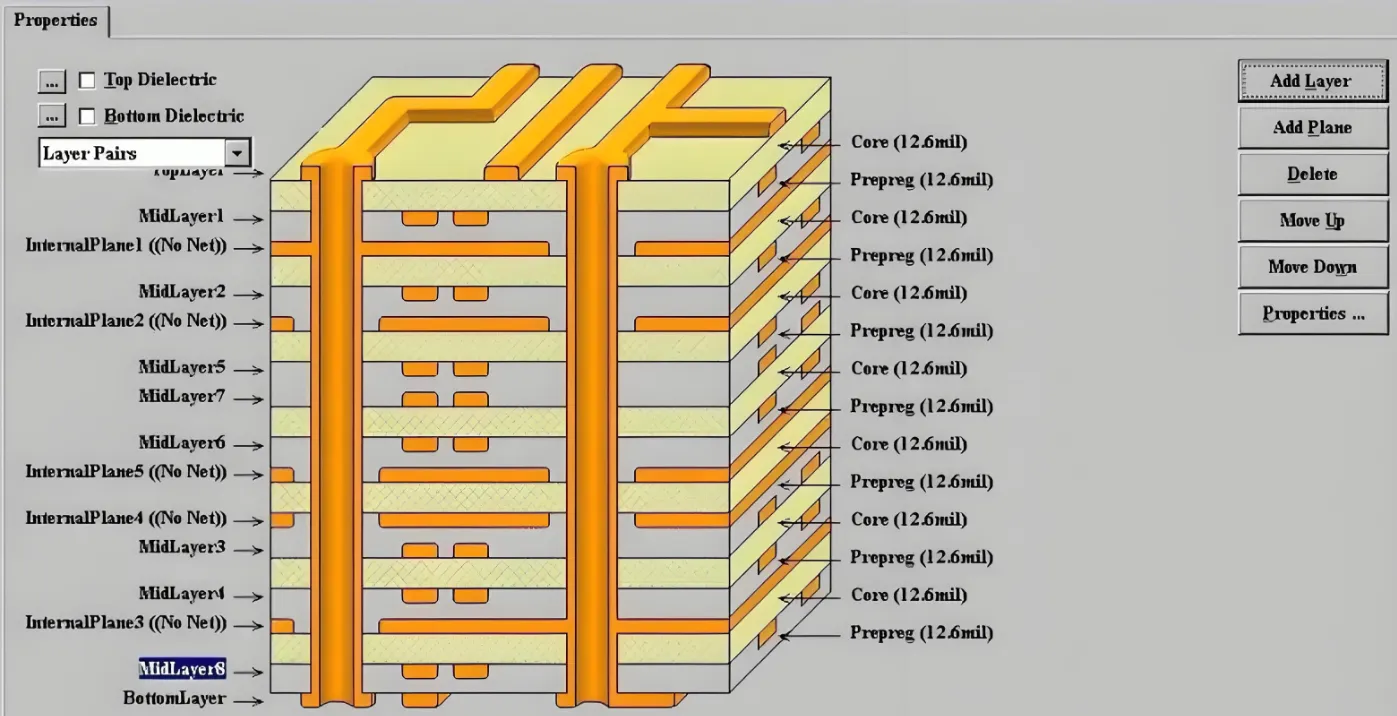
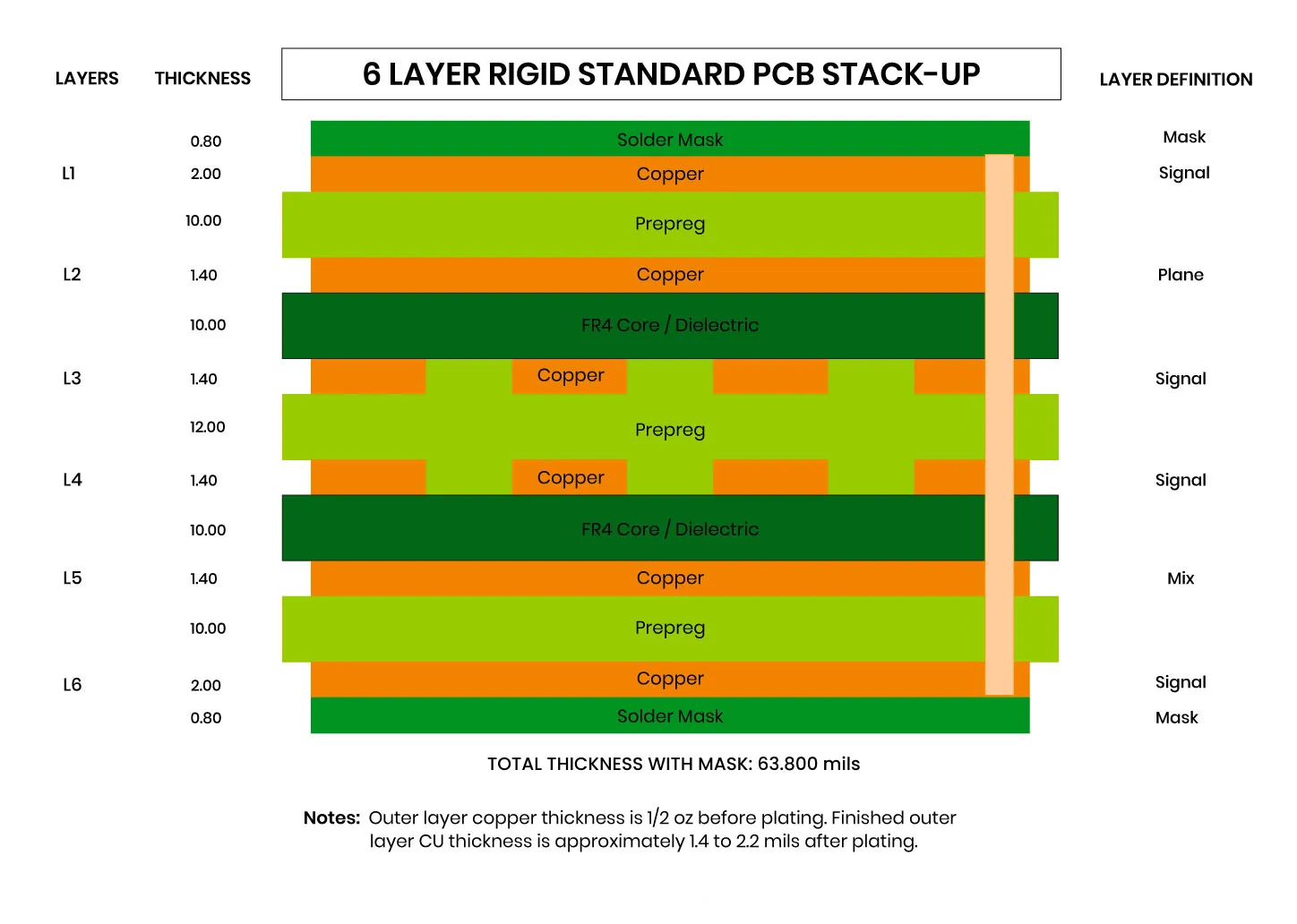
- Stack-up Complexity: In multilayer boards with 8 or more layers, multiple prepreg layers are used, and cumulative thickness variations can compound, leading to greater impedance deviations.
To address these challenges, designers should collaborate closely with their PCB fabricator to define acceptable tolerances and select materials with stable properties. Advanced manufacturing processes, such as laser-drilled microvias and precise lamination techniques, can also help maintain consistent prepreg thickness.
Practical Tips for Designing Controlled Impedance PCBs
Designing a controlled impedance PCB with optimal prepreg thickness requires careful planning and coordination. Here are some actionable tips to guide you through the process:
- Define Impedance Requirements Early: Specify the target impedance (e.g., 50Ω for single-ended lines) at the start of your design. Use this value to guide your stack-up and material choices.
- Select the Right Prepreg Material: Choose prepreg with a known dielectric constant and thickness tolerance. For high-frequency applications, consider low-loss materials with dielectric constants below 3.5.
- Use Simulation Tools: Leverage PCB design software with built-in impedance calculators to model the effects of prepreg thickness on microstrip and stripline impedance. Adjust trace widths and layer spacing as needed.
- Communicate with Your Fabricator: Provide detailed stack-up drawings and impedance specifications to your PCB manufacturer. Request test coupons or impedance measurements on production boards to verify results.
- Account for Manufacturing Tolerances: Design with a buffer for variations in prepreg thickness, typically ±10%. If tighter control is needed, opt for premium materials or processes.
By following these steps, you can minimize the risk of impedance mismatches and ensure your PCB performs reliably in high-speed applications.
The Broader Impact of Prepreg Thickness on Signal Integrity
Beyond impedance control, prepreg thickness influences other aspects of signal integrity in a PCB. For instance, thicker prepreg layers can increase signal propagation delay due to the longer distance signals must travel through the dielectric. In a high-speed design operating at 10 Gbps, a 2-mil increase in prepreg thickness could add several picoseconds of delay, potentially affecting timing margins.
Additionally, prepreg thickness affects crosstalk between adjacent traces. Thinner dielectrics bring traces closer to ground planes, increasing capacitance and reducing crosstalk, but they also raise the risk of impedance being too high if not calculated correctly. Balancing these factors is essential for achieving optimal performance in densely packed boards.
Conclusion: Mastering Prepreg Thickness for Better PCB Impedance Control
The relationship between prepreg thickness and PCB impedance control is a fundamental consideration for any engineer working on high-frequency or high-speed designs. Whether you're dealing with microstrip impedance on the outer layers or stripline impedance in internal layers, the thickness of the dielectric material directly impacts the characteristic impedance of your transmission lines. Small variations can lead to significant performance issues, making precision and collaboration with your fabricator critical.
By understanding how prepreg thickness influences impedance and signal integrity, and by applying the practical tips outlined in this guide, you can design controlled impedance PCBs that meet the stringent demands of modern electronics. From selecting the right materials to using simulation tools and accounting for manufacturing tolerances, every step counts in achieving reliable and efficient circuit performance.
At ALLPCB, we're committed to supporting engineers with the tools and expertise needed to navigate these complex design challenges. With a focus on precision manufacturing and high-quality materials, we help ensure your PCBs meet the exacting standards of impedance control and beyond.


