In high-speed PCB design, even the smallest oversight can lead to big problems. One often underestimated factor is line width tolerance. Ignoring it can result in costly signal integrity issues, reduced manufacturing yield, and expensive redesigns. So, what are the hidden costs of neglecting PCB line width tolerance? Simply put, it can lead to signal distortion, impedance mismatches, and production failures, all of which increase expenses and delay projects.
In this blog, we’ll dive deep into why line width tolerance matters in high-speed PCB design. We’ll explore its impact on signal integrity, impedance control, and manufacturing yield, while uncovering the financial and performance costs of ignoring this critical detail. Whether you’re an engineer or a project manager, understanding these factors can save you time and money.
Why Line Width Tolerance Matters in High-Speed PCB Design
In high-speed PCB design, every detail counts. Line width tolerance refers to the allowable variation in the width of traces on a printed circuit board during manufacturing. For standard designs, a tolerance of ±10% might be acceptable. But in high-speed applications, where signals travel at gigahertz frequencies, even a 1% deviation can disrupt performance.
High-speed signals, such as those in USB 3.0 (5 Gbps) or PCIe 4.0 (16 Gbps), are extremely sensitive to trace dimensions. A trace that’s too narrow or too wide can alter the electrical characteristics, leading to problems like signal reflection or crosstalk. These issues don’t just affect performance—they can also lead to costly redesigns or production delays.

The Role of Line Width in Signal Integrity
Signal integrity is the foundation of reliable high-speed PCB performance. It ensures that signals travel from source to destination without distortion, noise, or timing errors. Line width plays a critical role in maintaining signal integrity because it directly affects the electrical properties of the trace.
For instance, a trace that’s too narrow increases resistance, causing voltage drops and heat buildup. On the other hand, a trace that’s too wide can lead to unexpected capacitance, slowing down signal propagation. In a high-speed design operating at 10 GHz, a mere 0.1 mil (2.54 micrometers) deviation in line width can cause significant signal degradation.
Poor signal integrity often results in data errors or system failures. Imagine a telecommunications board failing to transmit data accurately due to signal distortion. The cost of debugging and fixing such issues can quickly add up, not to mention the potential loss of customer trust.
Impedance Control and Line Width Tolerance
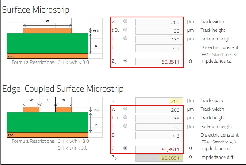
Impedance control is another crucial aspect of high-speed PCB design, and it’s closely tied to line width tolerance. Impedance, measured in ohms, determines how a signal travels through a trace. Most high-speed designs, like those for DDR4 memory (50-60 ohms) or HDMI (100 ohms differential), require precise impedance matching to avoid reflections and signal loss.
Line width directly impacts characteristic impedance. A wider trace lowers impedance, while a narrower trace increases it. If manufacturing tolerances are not tight enough—say, a ±5% variation instead of the required ±2%—the impedance can fall outside the acceptable range. For example, a target impedance of 50 ohms might vary between 47.5 and 52.5 ohms with a ±5% tolerance, potentially causing signal mismatch.
The cost of impedance mismatches isn’t just technical—it’s financial. Boards that fail impedance testing often need to be scrapped or reworked, driving up production costs. In extreme cases, entire batches may be rejected, leading to significant losses in time and resources.

Manufacturing Yield: The Silent Cost of Loose Tolerances
Manufacturing yield is the percentage of usable boards produced in a batch. In high-speed PCB production, maintaining tight line width tolerances is essential for achieving a high yield. If tolerances are too loose, more boards will fail quality checks due to signal integrity or impedance issues.
For example, let’s say a manufacturer produces 1,000 high-speed boards with a line width tolerance of ±10%. If 10% of the boards fail due to trace variations, that’s 100 unusable units. At a cost of $50 per board, the financial loss is $5,000—not counting the time spent on rework or replacement. Tightening the tolerance to ±2% might increase upfront manufacturing costs slightly, but it could reduce failure rates to 2%, saving thousands in the long run.
Low manufacturing yield also delays project timelines. If a batch fails quality control, you’ll need to wait for a new production run, pushing back product launches and potentially missing market opportunities. For industries like consumer electronics or automotive, where timing is critical, these delays can be catastrophic.
The Financial Impact of Ignoring Line Width Tolerance
The hidden costs of ignoring line width tolerance in high-speed PCBs go beyond technical failures. Let’s break down the financial impact across different stages of the design and production process.
1. Design and Prototyping Costs
During the design phase, failing to account for line width tolerance can lead to multiple prototype iterations. Each round of prototyping costs money—often hundreds or thousands of dollars per batch. If a design flaw caused by improper tolerance specifications is only discovered after the first prototype, you’re looking at additional expenses for redesign and retesting.
2. Production Losses
As mentioned earlier, poor manufacturing yield directly translates to financial losses. Scrapped boards, rework, and overtime labor all add up. For high-volume production, even a 1% decrease in yield can result in significant costs. For instance, losing 1% of a 10,000-unit batch at $30 per board means a $3,000 loss.
3. Field Failures and Warranty Claims
If defective boards make it to the end product, the costs skyrocket. Field failures—where a product malfunctions after reaching the customer—can lead to warranty claims, returns, and even lawsuits. Replacing a single failed unit might cost $100 or more, and the damage to your brand’s reputation is immeasurable.
How to Mitigate the Risks of Line Width Tolerance Issues
Understanding the costs of ignoring line width tolerance is the first step. The next is taking action to minimize these risks. Here are practical strategies to ensure your high-speed PCB designs stay on track.
1. Specify Tight Tolerances in Design
Work closely with your design team to define precise line width tolerances based on the application. For high-speed designs, aim for tolerances of ±2% or better. Use simulation tools to predict how variations might affect signal integrity and impedance before sending the design to manufacturing.
2. Partner with Reliable Manufacturers
Choose a manufacturing partner with advanced equipment and strict quality control processes. Ensure they can meet the tight tolerances required for high-speed designs. Request detailed reports on line width variations during production to catch issues early.
3. Test and Validate Early
Invest in thorough testing during the prototyping phase. Use tools like Time Domain Reflectometry (TDR) to measure impedance and identify deviations in line width. Catching problems early reduces the risk of costly production failures.
4. Factor Tolerances into Cost Estimates
When budgeting for a project, account for the higher costs of tight tolerances. While tighter tolerances may increase manufacturing expenses by 10-20%, the savings from fewer failures and redesigns often outweigh the initial investment.
Real-World Examples of Line Width Tolerance Impact
To drive home the importance of line width tolerance, let’s look at a couple of hypothetical scenarios inspired by common industry challenges.
In one case, a company designing a 5G communication board ignored line width tolerance during the initial design phase. They opted for a standard ±10% tolerance to save on upfront costs. During testing, they discovered that over 15% of the boards failed impedance checks, leading to a $20,000 loss in scrapped units and a three-month delay in product launch.
In contrast, another company working on a high-speed data storage device specified a ±1% tolerance from the start. While their manufacturing costs were 15% higher, their failure rate was under 1%, saving them from expensive rework and ensuring an on-time release.
These examples highlight how a small investment in precision can prevent much larger losses down the line.
Conclusion: Don’t Underestimate Line Width Tolerance
In high-speed PCB design, ignoring line width tolerance is a gamble that rarely pays off. The hidden costs—ranging from signal integrity issues and impedance mismatches to reduced manufacturing yield and financial losses—can derail even the most well-planned projects. By prioritizing precision, specifying tight tolerances, and partnering with capable manufacturers, you can avoid these pitfalls and ensure reliable, high-performing boards.
At ALLPCB, we understand the critical role that line width tolerance plays in high-speed designs. Our advanced manufacturing processes and rigorous quality control help you achieve the precision your projects demand, minimizing risks and maximizing value. Whether you’re working on cutting-edge telecommunications or consumer electronics, paying attention to the smallest details like line width tolerance can make all the difference.
 ALLPCB


