ALLPCB


Developing sensors for smart city applications requires efficient and budget-friendly solutions, especially when it comes to PCB prototyping. If you're searching for ways to reduce PCB prototyping cost, achieve quick turn PCB results, or explore DIY PCB fabrication, you're in the right place. This blog will guide you through affordable methods and practical tips to create high-quality PCB prototypes for smart city sensor systems, ensuring your projects stay on track and within budget.
In the following sections, we’ll dive deep into various PCB prototype methods, highlight affordable PCB services, and provide actionable advice tailored for engineers and developers working on smart city innovations. Whether you're building sensors for traffic monitoring, environmental tracking, or energy management, these techniques will help you save time and money.
Why Low-Cost PCB Prototyping Matters for Smart City Sensors
Smart city sensor development is at the heart of modern urban planning, enabling data-driven solutions for traffic control, air quality monitoring, and energy efficiency. However, creating these sensors often involves multiple iterations of PCB designs to ensure accuracy and reliability. High prototyping costs can slow down innovation, especially for startups or small teams with limited budgets.
By focusing on low-cost PCB prototyping, you can test and refine sensor designs without breaking the bank. Affordable prototyping also allows for faster experimentation, which is critical when developing systems that need to handle real-time data with minimal latency—often requiring signal speeds above 100 MHz for high-frequency applications. Reducing PCB prototyping cost while maintaining quality ensures that smart city projects remain feasible and scalable.
Understanding PCB Prototyping Costs and How to Minimize Them
The PCB prototyping cost can vary widely based on factors like board size, layer count, and turnaround time. For a simple two-layer board of 10 cm x 10 cm, costs might range from $10 to $50 for a small batch, while complex multi-layer designs for high-speed sensors could climb to $100 or more per prototype. Additional expenses, such as shipping or expedited services for quick turn PCB orders, can further increase the total.
To minimize these costs, consider the following strategies:
- Optimize Your Design Early: Use simulation tools to test your PCB layout before fabrication. This reduces the need for multiple physical prototypes, saving both time and money.
- Start with Smaller Batches: Order only 5-10 units for initial testing rather than larger quantities. Many services offer competitive pricing for small runs.
- Choose Standard Materials: Opt for standard FR-4 material instead of specialized substrates unless your smart city sensor requires high-frequency performance (e.g., above 1 GHz) or unique thermal properties.
By focusing on these cost-saving measures, you can keep your budget in check while still producing functional prototypes for sensor testing.
Quick Turn PCB: Balancing Speed and Affordability
When working on smart city sensor projects, time is often as critical as cost. Quick turn PCB services allow you to receive prototypes in as little as 24-48 hours, which is essential for rapid iteration and meeting tight project deadlines. However, faster turnaround times often come with a premium price tag.
To balance speed and affordability:
- Prioritize Local or Regional Services: Choosing a manufacturer closer to your location can reduce shipping times and costs, ensuring faster delivery without the high fees of express options.
- Plan Ahead for Deadlines: If possible, build buffer time into your project schedule to avoid last-minute rush orders that inflate costs.
- Use Online Quotation Tools: Many platforms provide instant pricing for different turnaround times, helping you select the most cost-effective option for your needs.
For smart city sensors, where testing and deployment timelines are often tight, mastering quick turn PCB strategies can make a significant difference in project success.
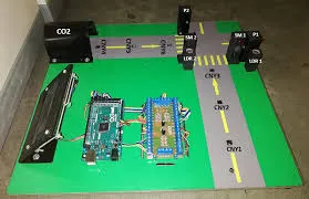
DIY PCB Fabrication: A Hands-On Approach for Cost Savings
For engineers who want maximum control over PCB prototyping cost, DIY PCB fabrication offers a viable alternative. This method is particularly useful for early-stage smart city sensor development, where you might need to test basic circuits before moving to professional manufacturing.
Here’s a step-by-step guide to DIY PCB fabrication:
- Design Your PCB: Use free or low-cost software to create your layout. Ensure your design accounts for the sensor’s power requirements (e.g., 3.3V or 5V) and signal integrity needs.
- Print the Layout: Transfer your design onto a copper-clad board using a laser printer and special transfer paper. The toner acts as a mask for etching.
- Etch the Board: Submerge the board in a chemical solution like ferric chloride to remove unprotected copper, leaving only your circuit traces. Handle chemicals with care and follow safety guidelines.
- Drill Holes: Use a small drill to create holes for through-hole components, ensuring precision for sensor ICs and connectors.
- Assemble and Test: Solder components onto the board and test the circuit for functionality, checking for issues like impedance mismatches (targeting around 50 ohms for RF sensors).
While DIY PCB fabrication can save money, it’s best suited for simple designs or single prototypes. For complex multi-layer boards or high-volume production, professional services are more reliable. Additionally, DIY methods can take longer and may not achieve the precision needed for high-frequency smart city sensors.
Affordable PCB Services: Finding the Right Partner
For those who prefer to outsource prototyping, selecting affordable PCB services is key to managing costs without sacrificing quality. Many providers cater to small-scale developers and offer competitive pricing for smart city sensor projects.
When choosing a service, keep these factors in mind:
- Low Minimum Order Quantities (MOQs): Look for providers that allow small batch orders (e.g., 5-10 boards) at reasonable prices, ideal for prototyping.
- Transparent Pricing: Opt for services with clear pricing structures, including costs for additional features like solder masks or silkscreen printing.
- Support for Sensor-Specific Needs: Ensure the provider can handle designs with tight tolerances, such as impedance control for high-speed data transmission (e.g., maintaining 50-ohm traces for RF applications).
By partnering with the right provider, you can access professional-grade prototypes at a fraction of the cost, allowing you to focus on refining your smart city sensor designs.
Popular PCB Prototype Methods for Smart City Sensors
There are several PCB prototype methods suited for smart city sensor development, each with its own advantages and cost implications. Below are the most common approaches:
1. Single-Sided and Double-Sided Boards
For basic sensors like temperature or humidity monitors, single-sided or double-sided PCBs are often sufficient. These are the most cost-effective options, with prices as low as $1-2 per board for small batches. They work well for low-frequency applications (below 10 MHz) and simple power requirements.
2. Multi-Layer Boards
For more advanced sensors, such as those used in traffic monitoring or wireless communication, multi-layer boards (4-6 layers) are necessary to handle complex routing and high-speed signals (above 100 MHz). While more expensive, costing $20-50 per board, they offer better performance and noise reduction through dedicated ground planes.
3. Flexible and Rigid-Flex PCBs
In smart city applications where sensors need to fit into compact or irregular spaces (e.g., wearable environmental trackers), flexible or rigid-flex PCBs are ideal. These cost more (starting at $30 per board) but provide durability and adaptability for unique designs.
Choosing the right method depends on your sensor’s specific requirements, including signal speed, power consumption, and physical constraints. Always weigh the cost against the performance needs of your project.
Best Practices for Designing PCBs for Smart City Sensors
Effective PCB design is the foundation of successful prototyping. Here are some best practices to ensure your smart city sensor PCBs are both functional and cost-efficient:
- Minimize Component Count: Reduce the number of components to lower assembly costs and simplify testing. For instance, use integrated sensor modules that combine multiple functions into a single chip.
- Focus on Signal Integrity: For high-speed sensors, maintain controlled impedance (e.g., 50 ohms for RF lines) and keep trace lengths short to avoid signal degradation.
- Include Test Points: Add test points in your design to simplify debugging and validation during prototyping. This reduces the risk of costly redesigns.
- Consider Power Efficiency: Smart city sensors often operate on battery power, so design for low power consumption (e.g., using 3.3V logic instead of 5V where possible).
Following these guidelines will help you create prototypes that meet performance standards while keeping PCB prototyping cost under control.
Conclusion: Building Smarter Cities with Affordable PCB Prototyping
Developing sensors for smart city applications doesn’t have to strain your budget. By leveraging low-cost PCB prototype methods, exploring DIY PCB fabrication, and partnering with affordable PCB services, you can bring innovative solutions to life without overspending. Whether you need quick turn PCB options for tight deadlines or want to minimize PCB prototyping cost through strategic design, the techniques covered in this blog provide a roadmap for success.
Start by assessing your project’s specific needs—signal speed, power requirements, and physical constraints—and choose the prototyping approach that best aligns with your goals. With the right strategies, you can accelerate smart city sensor development and contribute to building more connected, efficient urban environments.