 ALLPCB


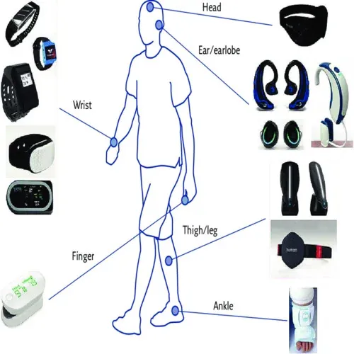
In the rapidly evolving world of healthcare technology, wearable health monitors are transforming how we track and manage personal wellness. From smartwatches that measure heart rate to patches that monitor glucose levels, these devices rely heavily on cutting-edge printed circuit board (PCB) design and manufacturing. So, what does the future hold for wearable health monitors, and how are innovations in PCB technology driving this change? In this blog, we’ll dive deep into the advancements shaping the industry, focusing on future PCB technology for wearables, advanced PCB materials, 3D printing PCBs, flexible hybrid electronics, and PCB trends in medical devices.
Why PCB Innovation Matters for Wearable Health Monitors
Wearable health monitors are becoming essential tools for both individuals and healthcare professionals. These devices need to be small, lightweight, durable, and capable of delivering precise data in real-time. At the heart of every wearable device lies a PCB, the foundation that connects sensors, processors, and power systems. As the demand for more advanced wearables grows, PCB design and manufacturing must evolve to meet challenges like size constraints, power efficiency, and biocompatibility.
Innovations in PCB technology are enabling wearables to become more comfortable, accurate, and versatile. Whether it’s a fitness tracker or a medical-grade device monitoring vital signs, the future of these tools depends on smarter, more efficient PCB solutions. Let’s explore the key trends and technologies shaping this exciting field.
Future PCB Technology for Wearables: Smaller, Smarter, and More Efficient
The future of PCB technology for wearables is centered on miniaturization and performance. As wearables shrink in size to improve user comfort, PCBs must pack more functionality into smaller footprints. High-density interconnect (HDI) PCBs are becoming a go-to solution, allowing for finer traces and smaller vias. For instance, HDI designs can achieve trace widths as small as 50 micrometers, enabling complex circuits in devices no larger than a coin.
Moreover, power efficiency is critical for wearables, which often run on tiny batteries. Advanced PCB layouts are being optimized to reduce power loss, with some designs cutting energy consumption by up to 30% through better thermal management and signal integrity. This means longer battery life for devices like heart rate monitors, ensuring they can operate for days without a recharge.
Signal speed is another area of focus. Wearable health monitors rely on fast, accurate data transmission to provide real-time feedback. Modern PCBs are being designed with impedance control, maintaining consistent signal paths with impedance values often targeted at 50 ohms for high-speed applications. This ensures minimal data loss, which is crucial for medical devices tracking critical metrics like blood oxygen levels.
Advanced PCB Materials: Enhancing Durability and Biocompatibility
The materials used in PCB manufacturing are evolving to meet the unique demands of wearable health monitors. Traditional rigid boards made from FR-4 are giving way to advanced materials that offer flexibility, durability, and safety for skin contact. Polyimide, for example, is a popular choice for flexible PCBs due to its excellent thermal stability and ability to withstand repeated bending without cracking. This material can endure temperatures up to 260°C, making it ideal for wearables exposed to varying environmental conditions.
For medical-grade wearables, biocompatibility is a top priority. PCBs must be safe for prolonged skin contact, avoiding materials that could cause irritation or allergic reactions. Some manufacturers are turning to specialized coatings and substrates, like medical-grade silicones, to ensure safety. Additionally, research is underway to develop eco-friendly PCB materials, reducing the environmental impact of wearable tech production.
Conductive inks and nanomaterials are also gaining traction. These materials allow for the creation of ultra-thin, lightweight circuits that conform to the body’s contours. For instance, silver nanoparticle inks can be used to print circuits with conductivity levels comparable to traditional copper traces, opening new possibilities for seamless integration into clothing or skin-adhering patches.
3D Printing PCBs: Revolutionizing Design and Production
3D printing technology is making waves in PCB manufacturing, offering a faster, more customizable approach to creating circuits for wearable health monitors. Unlike traditional methods that involve multiple steps like etching and drilling, 3D printing allows for the direct deposition of conductive and insulating layers, reducing production time by as much as 50% in some cases.
For wearables, 3D-printed PCBs enable complex, non-planar designs that can fit into irregular shapes, such as curved wristbands or contoured patches. This technology also supports rapid prototyping, allowing engineers to test and refine designs quickly. Imagine a scenario where a medical device manufacturer prints a custom PCB for a patient-specific wearable monitor in just a few hours—3D printing makes this possible.
Moreover, 3D printing can integrate multiple components into a single structure, reducing the need for separate assembly steps. This not only cuts costs but also improves reliability by minimizing connection points that could fail. While still in its early stages for mass production, 3D printing is poised to become a cornerstone of future PCB technology for wearables, especially as materials and precision continue to improve.
Flexible Hybrid Electronics: Merging Comfort with Functionality
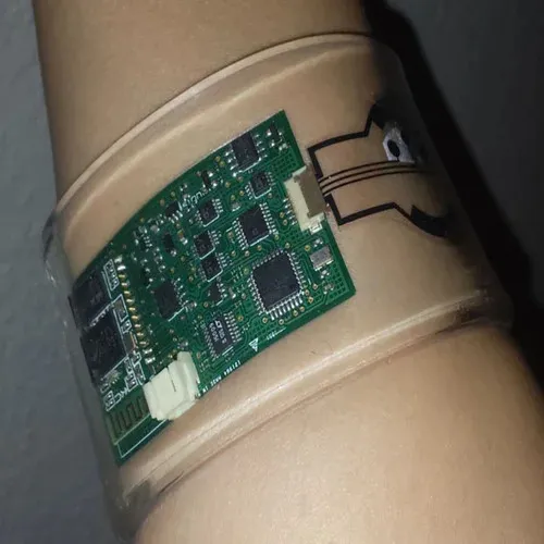
Flexible hybrid electronics (FHE) represent a groundbreaking shift in PCB design for wearable health monitors. FHE combines the flexibility of printed electronics with the performance of traditional rigid components, creating systems that are both adaptable and powerful. This technology is ideal for devices that need to bend and stretch with the body, such as skin patches or smart textiles.
One of the standout benefits of FHE is its ability to integrate sensors directly into the circuit. For example, a flexible PCB in a health monitor can embed pressure or temperature sensors without adding bulk, ensuring the device remains lightweight—often under 10 grams. This is a game-changer for patient comfort, especially for long-term monitoring applications like continuous glucose tracking.
FHE also supports the use of stretchable substrates, which can elongate by up to 30% without losing conductivity. This durability is essential for wearables that endure constant movement, ensuring reliable performance over time. As FHE technology advances, we can expect to see more seamless integration of electronics into everyday items, blurring the line between technology and fashion.
PCB Trends in Medical Devices: Meeting Stringent Standards
The use of PCBs in medical devices, including wearable health monitors, is guided by strict regulatory standards and performance requirements. Reliability is non-negotiable— a failure in a PCB could lead to inaccurate readings or even endanger a patient’s health. As a result, PCB trends in medical devices focus on precision, safety, and data security.
One key trend is the adoption of multi-layer PCBs to handle the complexity of medical wearables. These boards can have 8 or more layers, allowing for dense component placement while maintaining signal integrity. This is particularly important for devices that process multiple data streams, such as heart rate, temperature, and motion, all at once.
Another trend is the integration of wireless connectivity directly into PCB designs. Wearable health monitors increasingly rely on Bluetooth or Wi-Fi to transmit data to smartphones or cloud systems for analysis. PCBs are now being designed with built-in antennas, reducing the need for external components and keeping devices compact. For instance, a typical Bluetooth-enabled PCB can achieve data transfer rates of up to 2 Mbps, ensuring quick and reliable communication.
Finally, cybersecurity is becoming a critical consideration. With wearable health monitors collecting sensitive personal data, PCBs must incorporate encryption and secure data pathways to prevent breaches. This often involves dedicated hardware security modules embedded in the PCB, adding an extra layer of protection without compromising performance.
Challenges and Opportunities in PCB Design for Wearables
While the future of PCB technology for wearable health monitors is bright, there are challenges to overcome. Manufacturing flexible and hybrid PCBs at scale can be costly, and ensuring consistent quality across batches remains a hurdle. Additionally, balancing power efficiency with performance in tiny devices requires ongoing innovation in design and materials.
However, these challenges also present opportunities. Advances in automation and AI-driven design tools are streamlining PCB development, reducing errors, and cutting costs. For example, simulation software can predict signal interference or thermal issues before production, saving time and resources. As these tools become more accessible, smaller companies can enter the wearable health market, driving further innovation.
The growing demand for personalized healthcare solutions also opens doors for custom PCB designs. Tailored wearables that address specific medical conditions, like arrhythmia or sleep apnea, are on the rise, and PCBs will play a central role in making these devices both effective and affordable.
How These Innovations Benefit End Users
For everyday users and healthcare providers, the advancements in PCB design and manufacturing translate to tangible benefits. Wearable health monitors are becoming more accurate, with sensors delivering data within a 1-2% margin of error for metrics like heart rate or blood pressure. They’re also more comfortable, thanks to flexible materials that mold to the body without causing discomfort.
Additionally, the extended battery life and wireless capabilities mean users can wear these devices for longer periods without interruption, providing continuous health insights. For medical professionals, the real-time data and secure transmission enabled by modern PCBs allow for better remote monitoring and quicker interventions, improving patient outcomes.
Conclusion: A New Era for Wearable Health Monitors
The future of wearable health monitors is intertwined with the evolution of PCB design and manufacturing. From future PCB technology for wearables to the use of advanced materials, 3D printing, flexible hybrid electronics, and emerging PCB trends in medical devices, every aspect of PCB innovation is pushing the boundaries of what these tools can achieve. As technology continues to advance, we can look forward to wearables that are not only more powerful and precise but also more accessible to people worldwide.
At ALLPCB, we’re committed to supporting this transformation by providing cutting-edge solutions for PCB design and production. Whether you’re developing the next big wearable health monitor or exploring new medical device applications, our expertise and resources are here to help bring your vision to life.


