Designing a printed circuit board (PCB) for robotics control systems demands precision and attention to detail to ensure optimal performance. Whether you're working on a robotic arm, autonomous vehicle, or industrial automation system, the PCB layout can make or break your project. In this comprehensive guide, we’ll explore the best practices for PCB layout, routing, component placement, ground planes, power planes, impedance control, and thermal management to help you achieve a reliable and efficient design.
If you’re looking for a quick answer, the key to a high-performing robotics control PCB lies in careful planning: prioritize component placement for signal integrity, use dedicated ground and power planes to minimize noise, control impedance for high-speed signals, and manage heat dissipation to prevent failures. Now, let’s dive deeper into each aspect with actionable tips and detailed guidelines to elevate your PCB design process.
Why PCB Layout Matters for Robotics Control Systems
In robotics, control systems manage motors, sensors, microcontrollers, and communication modules, often operating in real-time with high-speed signals. A poorly designed PCB can lead to issues like electromagnetic interference (EMI), signal delays, or overheating, causing erratic behavior or system failure. A well-thought-out PCB layout ensures reliable operation, reduces noise, and extends the lifespan of your robotic system.

1. Component Placement: Building the Foundation
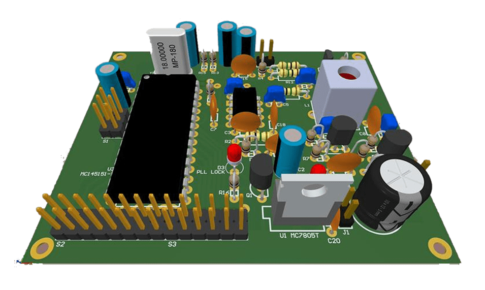
Component placement is the first step in PCB layout design and sets the stage for routing and overall performance. In robotics control systems, components like microcontrollers, power regulators, motor drivers, and sensors must be positioned strategically to minimize signal interference and optimize functionality.
- Group by Function: Place related components, such as a microcontroller and its supporting capacitors, close together to reduce trace lengths and noise. For example, keep decoupling capacitors within 0.1 inches (2.54 mm) of the power pins of ICs.
- Prioritize High-Speed Components: Position high-speed components like communication modules (e.g., for CAN bus or Ethernet) away from noisy elements like motor drivers to avoid crosstalk.
- Consider Mechanical Constraints: Ensure connectors and sensors are placed near the board's edges for easy access in a robotic assembly. Account for the physical size of components to avoid overcrowding.
2. Routing: Ensuring Signal Integrity
Routing, or the process of connecting components with traces, is critical for maintaining signal integrity in robotics control PCBs. Poor routing can introduce delays, noise, or even complete signal failure, especially in high-speed or high-power applications.
- Keep Traces Short and Direct: Minimize the length of critical signal traces, especially for high-speed data lines. For instance, USB or SPI signals should have traces shorter than 6 inches (15 cm) whenever possible to avoid signal degradation.
- Avoid 90-Degree Angles: Use 45-degree angles or curved traces to prevent signal reflection and EMI. Sharp corners can act as antennas, radiating unwanted noise.
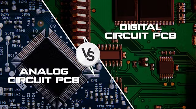
- Separate Analog and Digital Signals: Route analog signals (like sensor inputs) away from digital signals (like clock lines) to prevent interference. Maintain at least a 20-mil (0.5 mm) separation between these traces.
3. Ground Planes: Reducing Noise and EMI
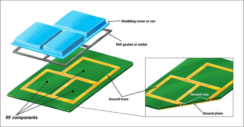
A solid ground plane is essential for minimizing noise and ensuring stable operation in robotics control systems. Ground planes provide a low-impedance path for return currents, reducing the risk of EMI and crosstalk.
- Use a Continuous Ground Plane: Dedicate an entire layer to a ground plane in multilayer PCBs. Avoid splitting the ground plane unless absolutely necessary, as splits can create ground loops and increase noise.
- Connect Ground Pins Properly: Ensure all ground pins of ICs and components are connected to the ground plane with vias. For high-frequency components, use multiple vias to reduce inductance.
- Star Grounding for Analog Circuits: In mixed-signal designs, consider a star grounding approach where analog and digital grounds meet at a single point to prevent noise coupling.
4. Power Planes: Delivering Stable Voltage
Power planes are just as important as ground planes in robotics control PCBs, especially since robotic systems often require multiple voltage levels for different components (e.g., 3.3V for microcontrollers, 12V for motors).
- Dedicate Layers for Power: In multilayer designs, assign specific layers to power planes to ensure low impedance and stable voltage distribution. For instance, a 4-layer board might have layer 2 as a power plane and layer 3 as a ground plane.
- Use Decoupling Capacitors: Place decoupling capacitors (e.g., 0.1 μF ceramic capacitors) near power pins to filter out high-frequency noise. A general rule is one capacitor per power pin for ICs.
- Minimize Voltage Drops: Widen power traces or use power planes to handle high currents, especially for motor drivers that might draw 5A or more. Calculate trace width based on current using IPC-2221 standards to avoid overheating.
5. Impedance Control: Managing High-Speed Signals
Impedance control is crucial for high-speed signals in robotics control systems, such as those used in communication protocols like USB, Ethernet, or high-frequency sensor data. Mismatched impedance can cause signal reflections, leading to data errors or loss.
- Calculate Trace Impedance: Use tools or formulas to match trace impedance to the required value, typically 50 ohms for single-ended signals or 100 ohms for differential pairs. Adjust trace width and spacing based on the PCB stack-up and dielectric constant (e.g., FR4 has a dielectric constant of about 4.5).
- Maintain Consistent Trace Width: Keep trace widths and spacing uniform for differential pairs to avoid impedance discontinuities. For example, a 5-mil (0.127 mm) trace with 5-mil spacing might be suitable for a 100-ohm differential pair on a standard FR4 board.
- Use Reference Planes: Route high-speed traces over a continuous ground plane to maintain controlled impedance and reduce EMI.
6. Thermal Management: Preventing Overheating
Robotics control PCBs often handle high currents for motors or power-hungry components, generating significant heat. Effective thermal management ensures reliability and prevents component failure.
- Use Thermal Vias: Place thermal vias under high-power components like motor drivers or voltage regulators to transfer heat to other layers or a heatsink. A grid of 10-15 vias with a 0.3 mm diameter can significantly improve heat dissipation.
- Add Copper Pours: Increase copper area around heat-generating components to act as a heat spreader. Ensure these areas are connected to ground or power planes for better thermal distribution.
- Consider Heatsinks: For components dissipating more than 1-2 watts, attach heatsinks or use PCB-mounted cooling solutions. Ensure adequate spacing for airflow in the robotic enclosure.
7. Additional Best Practices for Robotics PCB Layout
Beyond the core elements, a few additional practices can further enhance the performance of your robotics control PCB.
- Follow Design Rules: Adhere to design rules for trace width, spacing, and via sizes based on manufacturing capabilities. For example, many manufacturers recommend a minimum trace width of 6 mils (0.15 mm) for standard processes.
- Test Points and Debugging: Include test points for critical signals and power rails to simplify debugging and validation of the PCB after assembly.
- Simulate Before Fabrication: Use simulation tools to analyze signal integrity, power distribution, and thermal performance before sending your design for manufacturing. This can save time and reduce costly revisions.
Conclusion: Crafting High-Performance Robotics Control PCBs
Designing a PCB for robotics control systems is a complex but rewarding task. By focusing on strategic component placement, meticulous routing, robust ground and power planes, precise impedance control, and effective thermal management, you can create a board that performs reliably even in demanding applications. Each step, from initial layout to final simulation, plays a vital role in ensuring your robotic system operates at its best.
At ALLPCB, we’re committed to supporting engineers with resources and services to bring their designs to life. Whether you’re prototyping a new robotics controller or scaling up for production, following these PCB layout guidelines will help you achieve optimal performance and avoid common pitfalls. Start applying these best practices in your next project, and watch your designs reach new levels of efficiency and reliability.
 ALLPCB


