 ALLPCB


Designing a Printed Circuit Board (PCB) outline is a critical step in ensuring a seamless mechanical fit and integration into an enclosure or larger system. For engineers and designers, getting the PCB outline right means avoiding costly redesigns, ensuring proper connector placement, and achieving a secure fit with mounting holes. In this comprehensive guide, we’ll explore the best practices for PCB outline design, focusing on mechanical fit, enclosure integration, connector placement, and mounting holes. Whether you're a seasoned engineer or just starting, these tips will help you create reliable and efficient PCB designs.
Why PCB Outline Design Matters for Mechanical Fit and Integration
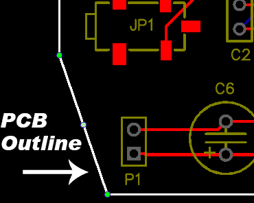
The PCB outline defines the physical shape and size of your board, directly impacting how it fits into an enclosure or connects with other components. A well-designed outline ensures that the board aligns perfectly with mounting points, connectors, and enclosure constraints, reducing the risk of mechanical stress or assembly issues. Poorly planned outlines can lead to misaligned connectors, insufficient clearance, or even board damage during installation. Let’s dive into the best practices to achieve an optimal PCB outline for mechanical fit and integration, targeting key aspects like enclosure design, connector placement, and mounting holes.
Key Elements of PCB Outline Design for Mechanical Fit
When designing a PCB outline for mechanical fit, precision is everything. The outline must match the intended enclosure or system dimensions to avoid gaps or interference. Here are some best practices to ensure a perfect fit:
- Define Clear Dimensions: Start by determining the exact dimensions of the space where the PCB will be installed. Use precise measurements, ideally in millimeters, to define the board’s length, width, and thickness. For example, if your enclosure has an internal dimension of 100mm x 50mm, ensure your PCB outline stays within these limits, leaving a clearance of at least 0.5mm on each side to account for manufacturing tolerances.
- Account for Manufacturing Tolerances: PCB fabrication processes have inherent tolerances, often ranging from ±0.1mm to ±0.2mm for outline dimensions. Design your outline with these tolerances in mind to prevent fit issues during assembly.
- Use Rounded Corners: Sharp corners can create stress points or complicate enclosure design. Opt for rounded corners with a radius of at least 1mm to improve structural integrity and ease of fit.
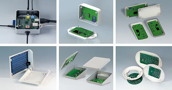
PCB Outline Enclosure Design: Ensuring Seamless Integration
Designing a PCB outline for enclosure integration requires careful planning to align the board with the enclosure’s internal features, such as standoffs, slots, and access points. A mismatch between the PCB and enclosure can lead to assembly delays or functional failures. Follow these tips for effective PCB outline enclosure design:
- Collaborate with Enclosure Specifications: Obtain the enclosure’s mechanical drawings or 3D models early in the design process. Match the PCB outline to the enclosure’s internal layout, ensuring alignment with mounting points and openings for connectors or displays.
- Plan for Clearance: Leave adequate clearance between the PCB edges and enclosure walls, typically 1-2mm, to prevent interference during installation and to accommodate thermal expansion. For high-power designs, consider additional space for heat dissipation.
- Consider Component Heights: The PCB outline should account for the tallest components on the board. Ensure the enclosure provides enough vertical clearance, especially for capacitors or heat sinks, to avoid contact or pressure points. For instance, if a component is 15mm tall, the enclosure should have at least 17mm of internal height to provide a safety margin.
- Design for Accessibility: Position cutouts or notches in the PCB outline to allow access to ports, buttons, or LEDs without removing the board from the enclosure. This enhances usability and simplifies maintenance.
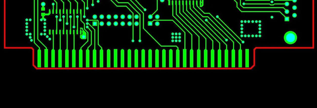
PCB Outline Connector Placement: Optimizing Functionality and Fit
Connector placement is a crucial aspect of PCB outline design, as it directly affects how the board interfaces with external systems. Misplaced connectors can lead to cable strain, poor accessibility, or mechanical misalignment. Here are some best practices for PCB outline connector placement:
- Position Connectors Near Edges: Place connectors along the edges of the PCB outline to simplify cable routing and minimize interference with other components. For example, USB or power connectors should be near the board’s perimeter to align with enclosure openings.
- Align with Enclosure Openings: Ensure connectors match the enclosure’s cutouts or slots. A mismatch, even by 1mm, can make assembly difficult or damage cables. Use mechanical drawings to confirm alignment during the design phase.
- Consider Cable Bend Radius: Account for the minimum bend radius of cables connected to the PCB. For instance, a typical USB cable may require a bend radius of at least 10mm. Ensure there’s enough space between the connector and adjacent components or enclosure walls to avoid stress on the cable.
- Secure Connectors Mechanically: For connectors subjected to frequent plugging and unplugging, add mechanical reinforcement like screws or brackets near the connector location on the PCB outline. This prevents stress on solder joints and extends the board’s lifespan.
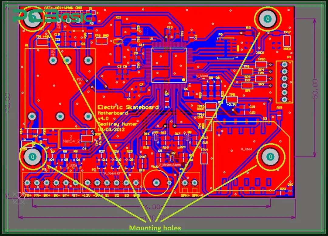
PCB Outline Mounting Holes: Ensuring Stability and Durability
Mounting holes are essential for securing a PCB within an enclosure or to a larger system. Properly designed mounting holes prevent movement, reduce mechanical stress, and ensure long-term reliability. Here’s how to optimize PCB outline mounting holes:
- Strategically Place Mounting Holes: Position mounting holes near the corners of the PCB outline to provide balanced support. For a rectangular board of 100mm x 50mm, place holes 5mm from each corner to maximize stability without compromising usable board space.
- Choose the Right Hole Size: Select a hole diameter that matches the screws or standoffs used in the enclosure. Common sizes range from 3mm to 4mm for M3 or M4 screws. Ensure the hole size includes a tolerance of +0.1mm to account for manufacturing variations.
- Add Annular Rings for Strength: Surround mounting holes with a copper annular ring (at least 0.5mm wide) to reinforce the hole and prevent cracking during assembly. Non-plated holes are often sufficient for mechanical mounting, but plated holes can be used if grounding is required.
- Keep Clear of Components: Maintain a clearance of at least 3mm between mounting holes and nearby components or traces to avoid interference during screw tightening or vibration. This also prevents accidental short circuits.
- Consider Vibration and Shock: In applications subject to vibration, such as automotive or industrial environments, add more mounting holes or use vibration-dampening materials. For a 150mm x 100mm board, consider six mounting holes instead of four for added stability.
Common Challenges in PCB Outline Design and How to Overcome Them
Even with careful planning, PCB outline design can present challenges. Here are some common issues related to mechanical fit, enclosure design, connector placement, and mounting holes, along with solutions:
- Issue: Misalignment with Enclosure: If the PCB outline doesn’t fit the enclosure, it may be due to inaccurate measurements or unaccounted tolerances. Solution: Always double-check enclosure dimensions using mechanical drawings and design with a clearance buffer of 0.5-1mm on all sides.
- Issue: Connector Accessibility Problems: Connectors that are hard to reach or misaligned with enclosure openings can frustrate assembly. Solution: Use 3D modeling tools to simulate the PCB and enclosure assembly, ensuring connectors align perfectly with cutouts.
- Issue: Insufficient Mounting Support: A PCB that shifts or vibrates in its enclosure often lacks proper mounting holes. Solution: Add additional holes or use larger screws (e.g., M4 instead of M3) for a more secure fit, especially in high-vibration environments.
- Issue: Component Interference: Tall components or poorly placed parts can clash with the enclosure or other boards. Solution: Map out component heights and positions early in the design phase, ensuring at least 2mm of vertical clearance above the tallest part.
Tools and Techniques for Perfecting Your PCB Outline Design
Modern design tools can significantly improve the accuracy of your PCB outline for mechanical fit and integration. Here are some techniques to leverage:
- Use CAD Software: Design software with 3D capabilities allows you to simulate the PCB outline within an enclosure, identifying fit issues before fabrication. Import enclosure models to verify alignment with connectors and mounting holes.
- Leverage Design Rule Checks (DRC): Set up DRC rules to enforce clearances around mounting holes (e.g., 3mm from components) and ensure the outline matches specified dimensions within tolerances.
- Prototype and Test: Before mass production, create a prototype to test the PCB outline’s fit in the actual enclosure. Check for connector alignment, mounting stability, and overall mechanical integration. Adjust the design based on test findings.
- Collaborate with Manufacturers: Work closely with your PCB fabrication and assembly partners to confirm that the outline design meets their capabilities. Provide detailed mechanical drawings with the outline, mounting holes, and connector positions clearly marked.
Final Thoughts on PCB Outline Best Practices
Achieving an optimal PCB outline for mechanical fit and integration is a balance of precision, foresight, and collaboration. By focusing on key areas like enclosure design, connector placement, and mounting holes, you can create a PCB that fits seamlessly into its intended environment, performs reliably, and withstands mechanical stresses. Remember to prioritize accurate measurements, account for tolerances, and use modern design tools to simulate and validate your outline before production. With these best practices, you’ll minimize design iterations, reduce costs, and deliver high-quality PCBs that meet both functional and mechanical requirements.
At ALLPCB, we’re committed to supporting engineers with resources and expertise to bring their designs to life. Whether you’re tackling complex enclosure integrations or fine-tuning connector placements, following these PCB outline best practices will set you up for success in every project.


