ALLPCB


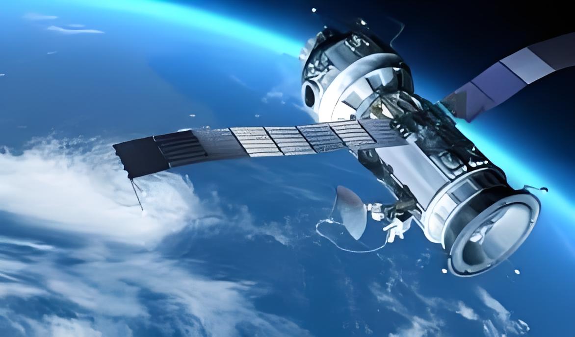
In the realm of spacecraft electronics, every inch of space counts. Miniaturization techniques for printed circuit boards (PCBs) are critical to maximizing space efficiency while maintaining high performance and reliability in the harsh conditions of space. At ALLPCB, we understand the unique challenges of designing electronics for spacecraft, where size, weight, and power constraints are paramount. This blog explores advanced strategies like high-density interconnect (HDI) PCB design, microvia technology for space, component miniaturization for PCBs, 3D PCB design for space, and advanced packaging techniques to help engineers achieve optimal results.
Whether you're designing electronics for satellites, probes, or crewed missions, this guide provides actionable insights into cutting-edge miniaturization methods. Let's dive into the details of how these techniques can transform spacecraft electronics and ensure mission success.
Why Miniaturization Matters in Spacecraft Electronics
Spacecraft operate under extreme limitations. The available space for electronics is often tiny, and every gram of weight impacts launch costs and fuel efficiency. Miniaturization of PCBs allows engineers to pack more functionality into smaller areas, reducing the overall size and weight of the spacecraft. This not only lowers costs but also improves mission capabilities by freeing up room for additional instruments or fuel.
Beyond size and weight, miniaturized electronics must withstand radiation, temperature extremes, and vacuum conditions. Techniques like HDI PCB design and advanced packaging ensure that these compact systems remain reliable. Let's explore the key methods driving miniaturization in spacecraft electronics.
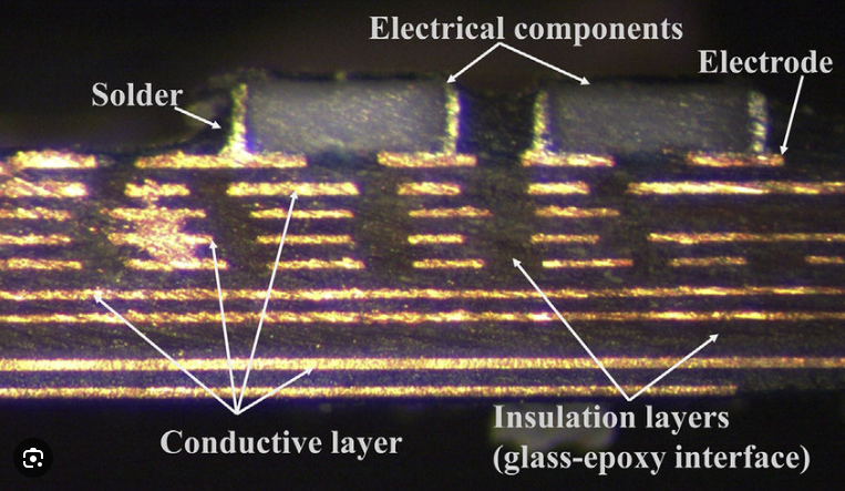
High-Density Interconnect (HDI) PCB Design: Packing More into Less
High-density interconnect (HDI) PCB design is a game-changer for spacecraft electronics. This technology enables finer lines, smaller vias, and denser component placement compared to traditional PCBs. By using multiple layers with intricate routing, HDI designs can support complex circuits in a fraction of the space.
For example, HDI boards often feature line widths and spacing as small as 3 mils (0.003 inches), allowing for a higher number of connections per square inch. This is crucial for spacecraft systems where microprocessors, sensors, and communication modules must coexist in tight quarters. Additionally, HDI reduces signal loss and crosstalk, improving performance at high frequencies—often critical for space communication systems operating at speeds exceeding 1 GHz.
HDI design also enhances thermal management, a vital consideration in space where heat dissipation is challenging due to the vacuum environment. By integrating more functionality into fewer layers, heat-generating components can be strategically placed to optimize cooling.
Microvia Technology for Space: Enabling Ultra-Compact Designs
Microvia technology is a cornerstone of HDI PCB design and a key enabler of miniaturization for space applications. Microvias are tiny holes, often less than 6 mils (0.006 inches) in diameter, that connect different layers of a PCB. Unlike traditional through-hole vias, microvias take up far less space, allowing for denser layouts and more efficient use of board real estate.
In spacecraft electronics, microvia technology for space is particularly valuable because it supports the integration of high-pin-count components like field-programmable gate arrays (FPGAs) and application-specific integrated circuits (ASICs). These components often require hundreds of connections, and microvias make it possible to route signals without increasing the board's footprint.
Moreover, microvias improve signal integrity by shortening connection paths, reducing impedance mismatches, and minimizing delays. For high-speed space applications, such as data transmission at rates of 10 Gbps or more, this can be a significant advantage. However, engineers must ensure that microvias are manufactured with precision to withstand the mechanical stresses of launch and the thermal cycling of space.
Component Miniaturization for PCBs: Shrinking the Building Blocks
Component miniaturization for PCBs focuses on reducing the size of individual electronic parts without sacrificing performance. In spacecraft design, smaller components mean more room for additional systems or redundancy, which is critical for mission reliability.
Modern surface-mount technology (SMT) has driven component sizes down to packages like 0201 (0.6 mm x 0.3 mm) for resistors and capacitors. These tiny parts allow for densely populated boards, but they require precise placement and soldering techniques to avoid defects. Additionally, integrated circuits (ICs) are increasingly available in wafer-level chip-scale packages (WLCSP), which eliminate the need for traditional packaging, further reducing size and weight.
For space applications, miniaturized components must also be radiation-hardened to resist cosmic rays and solar radiation. Engineers often select parts with a total ionizing dose (TID) tolerance of 100 krad or higher to ensure longevity in orbit. Balancing size reduction with durability is a constant challenge, but advancements in materials and testing are making it easier to achieve both.
3D PCB Design for Space: Thinking Beyond Flat Boards
Traditional flat PCBs are often insufficient for the tight constraints of spacecraft. 3D PCB design for space takes miniaturization to the next level by stacking layers or folding boards into three-dimensional configurations. This approach maximizes space efficiency by utilizing the vertical dimension, allowing for more components in a smaller footprint.
One common method is the use of rigid-flex PCBs, which combine rigid sections for component mounting with flexible sections that can be folded into compact shapes. For instance, a rigid-flex board might wrap around a spacecraft module, fitting into irregular spaces that a flat board couldn’t accommodate. This can reduce the overall volume of the electronics package by up to 50% in some designs.
Another emerging trend is 3D stacking of PCB layers using through-silicon vias (TSVs). This technique creates vertical interconnections between stacked chips or boards, enabling ultra-high-density designs. While TSVs are more complex and costly to implement, they offer unparalleled space savings and are ideal for high-performance computing systems in spacecraft, such as onboard data processing units handling terabytes of data per second.
Advanced Packaging Techniques: Integrating More in Less Space
Advanced packaging techniques are revolutionizing how electronics are assembled for spacecraft, pushing the boundaries of miniaturization. These methods focus on integrating multiple functions into a single package, reducing the need for separate components and interconnects.
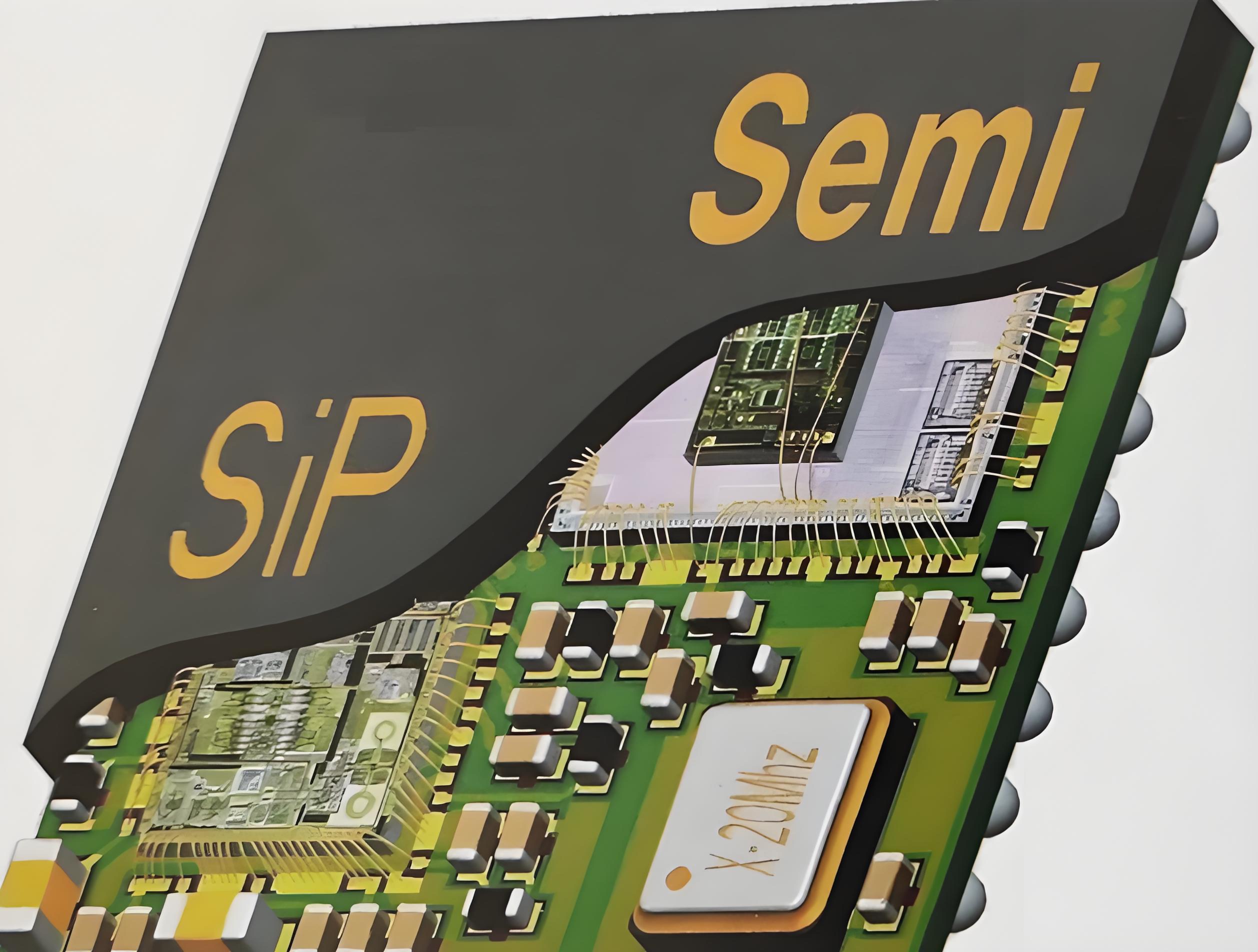
One prominent technique is system-in-package (SiP), which combines multiple chips—such as processors, memory, and sensors—into a single module. SiP can shrink the size of a system by 40% or more compared to traditional layouts, making it ideal for compact spacecraft electronics. It also reduces signal delay by minimizing the distance between chips, which is critical for high-speed applications.
Another approach is chip-on-board (CoB) packaging, where bare chips are directly mounted onto the PCB and sealed with a protective coating. This eliminates the bulk of traditional packaging, cutting down on both size and weight. CoB is particularly useful for LED arrays or sensor systems in spacecraft, where space is at a premium.
Lastly, 2.5D and 3D integrated circuit (IC) packaging use interposers and stacking to create dense, high-performance assemblies. These techniques can achieve interconnect densities exceeding 10,000 connections per square centimeter, supporting the complex requirements of modern space missions.
Challenges and Considerations in Miniaturization for Space
While miniaturization offers incredible benefits, it also comes with unique challenges. One major concern is thermal management. As components are packed closer together, heat dissipation becomes more difficult, especially in the vacuum of space where convection is nonexistent. Engineers must incorporate heat sinks, thermal vias, or advanced materials like ceramic substrates to manage temperatures effectively.
Another challenge is reliability. Smaller components and finer traces are more susceptible to mechanical stress during launch vibrations, which can reach accelerations of 10g or more. Rigorous testing, such as thermal cycling between -55°C and 125°C, and vibration testing, is essential to ensure that miniaturized PCBs can endure the rigors of space travel.
Signal integrity is also a concern in high-density designs. With traces and vias placed closer together, the risk of electromagnetic interference (EMI) increases. Careful design practices, such as controlled impedance routing (often targeting 50 ohms for high-speed signals), and the use of shielding can mitigate these issues.
Best Practices for Designing Miniaturized PCBs for Spacecraft
To achieve successful miniaturization, engineers should follow these best practices:
- Start with HDI and Microvia Integration: Use HDI PCB design and microvia technology to maximize routing density and minimize board size.
- Select Miniaturized, Space-Qualified Components: Opt for small-form-factor parts with proven radiation tolerance and reliability under space conditions.
- Explore 3D Configurations: Consider rigid-flex or stacked designs to utilize vertical space and fit into unconventional shapes.
- Leverage Advanced Packaging: Use SiP, CoB, or 3D IC packaging to integrate multiple functions into compact modules.
- Prioritize Testing: Conduct extensive environmental testing to validate the performance of miniaturized designs in space-like conditions.
Conclusion: The Future of Miniaturization in Spacecraft Electronics
Miniaturization techniques for spacecraft electronics PCBs are essential for meeting the demands of modern space missions. By adopting strategies like high-density interconnect (HDI) PCB design, microvia technology for space, component miniaturization for PCBs, 3D PCB design for space, and advanced packaging techniques, engineers can maximize space efficiency without compromising performance or reliability.
At ALLPCB, we are committed to supporting the aerospace industry with cutting-edge solutions for PCB design and manufacturing. As technology continues to evolve, we anticipate even smaller, more powerful electronics that will enable ambitious missions to explore deeper into the cosmos. By staying at the forefront of miniaturization trends, we help our clients achieve their goals in the challenging environment of space.