 ALLPCB


When it comes to designing high-density interconnect (HDI) printed circuit boards (PCBs), selecting the right microvia materials, especially dielectric materials, is crucial for ensuring optimal performance and reliability. Microvias are tiny holes that connect layers in HDI PCBs, and the dielectric material surrounding them impacts signal integrity, thermal management, and manufacturing ease. So, how do you choose the best dielectric for microvia applications? The answer lies in understanding the properties of laser drillable materials, balancing cost with performance, and prioritizing microvia reliability for your specific needs.
In this comprehensive guide, we’ll dive deep into the world of microvia materials and HDI PCB materials. We’ll explore the key characteristics of dielectric materials, the importance of laser drillable options, and how these choices affect microvia reliability. Whether you’re an engineer working on compact electronics or a designer aiming for high-speed performance, this blog will help you make informed decisions for your next project.
What Are Microvias and Why Do Materials Matter?
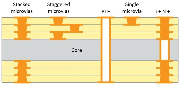
Microvias are small vias, typically less than 150 micrometers in diameter, used in HDI PCBs to connect multiple layers in a compact space. They are essential for modern electronics, enabling smaller, lighter, and faster devices like smartphones, wearables, and medical equipment. Unlike traditional through-hole vias, microvias are often created using laser drilling, which allows for precision and flexibility in design.
The materials used in and around microvias, particularly the dielectric layers, play a significant role in the performance of the PCB. Dielectric materials act as insulators between conductive layers, affecting signal speed, impedance, and heat dissipation. Choosing the wrong material can lead to issues like signal loss, poor thermal stability, or even manufacturing defects during laser drilling. That’s why understanding microvia materials and their properties is a critical step in HDI PCB design.
Key Properties of Dielectric Materials for Microvias
When selecting dielectric materials for microvia applications, several properties must be considered to ensure optimal performance. Let’s break down the most important factors:
1. Dielectric Constant (Dk)
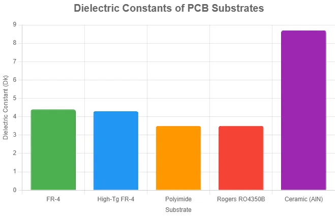
The dielectric constant, or Dk, measures how much a material can store electrical energy in an electric field. A lower Dk value means faster signal transmission, which is critical for high-speed applications. For example, standard FR-4 materials have a Dk of around 4.0 to 4.5, while advanced low-Dk materials can go as low as 2.5 to 3.0, improving signal integrity by reducing delays. For HDI PCBs with microvias, low-Dk dielectrics are often preferred to support high-frequency signals.
2. Dissipation Factor (Df)
The dissipation factor, or Df, indicates how much energy is lost as heat during signal transmission. A lower Df is better for minimizing signal loss, especially in high-frequency designs. Materials with a Df below 0.005 are ideal for microvia applications in high-speed electronics, as they reduce energy waste and maintain signal clarity.
3. Thermal Stability
During manufacturing and operation, PCBs are exposed to heat, which can cause materials to expand or degrade. Dielectric materials with high glass transition temperatures (Tg), typically above 150°C, are essential for maintaining structural integrity around microvias. This is especially important during laser drilling, as excessive heat can damage the material or affect hole quality.
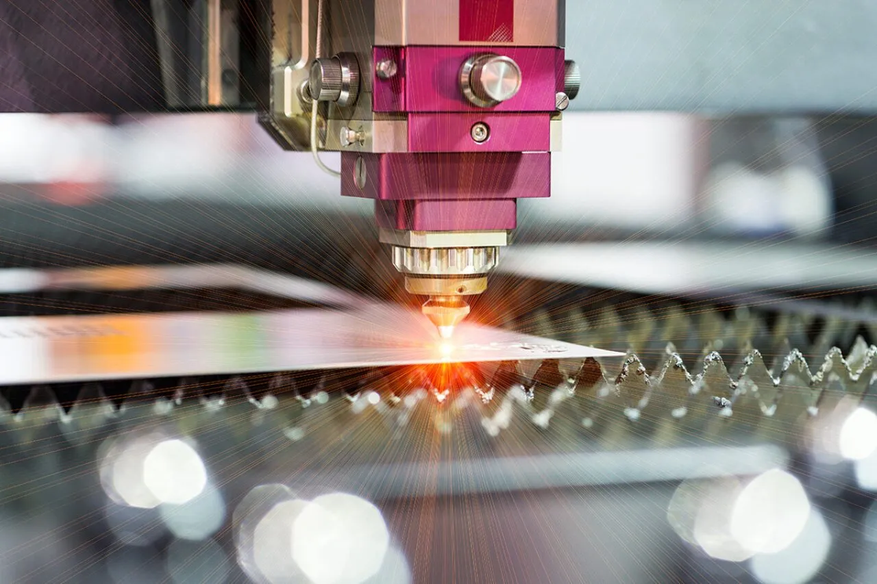
4. Laser Drillability
Not all dielectric materials are suitable for laser drilling, a common method for creating microvias. Laser drillable materials must have consistent composition and low filler content to ensure clean, precise holes without residue or uneven edges. Materials like resin-coated copper (RCC) or certain low-loss laminates are often chosen for their compatibility with laser processes.
Common Dielectric Materials for HDI PCB Microvias
There are several types of dielectric materials used in HDI PCBs, each with unique advantages and trade-offs. Below, we’ll explore some of the most common options for microvia applications.
1. FR-4 Based Materials
FR-4 is a widely used dielectric material made from woven fiberglass and epoxy resin. It’s cost-effective and offers decent mechanical strength, with a Dk of around 4.0 to 4.5. However, standard FR-4 may not be ideal for high-speed designs due to its higher signal loss and limited laser drillability. Enhanced versions of FR-4 with lower Dk and better thermal properties are sometimes used for budget-friendly HDI projects.
2. High-Performance Laminates
For applications requiring better signal integrity, high-performance laminates like polyimide or PTFE-based materials are popular. These materials have lower Dk values (around 2.5 to 3.5) and excellent thermal stability, making them suitable for high-frequency and high-temperature environments. They are also often laser drillable, though they come at a higher cost.
3. Resin-Coated Copper (RCC)
RCC is a thin dielectric layer coated with copper foil, commonly used in HDI PCBs for microvia formation. It is highly compatible with laser drilling, allowing for precise microvia creation. RCC typically has a moderate Dk of around 3.5, balancing performance and manufacturability for many applications.
4. Low-Loss Materials
Low-loss dielectrics, such as hydrocarbon-based or ceramic-filled materials, are designed for high-frequency applications. With Dk values as low as 2.2 and Df below 0.003, these materials minimize signal loss and are often used in telecommunications and aerospace industries. Their laser drillability varies, so compatibility with manufacturing processes must be verified.
Factors Affecting Microvia Reliability
Microvia reliability is a top concern in HDI PCB design, as failures can lead to costly rework or product malfunctions. The choice of dielectric material directly impacts reliability, along with other design and manufacturing factors. Here are the key aspects to consider:
1. Thermal Stress Resistance
During PCB assembly, components are soldered at high temperatures, causing thermal expansion. If the dielectric material around microvias cannot withstand this stress, cracks or delamination may occur. Studies have shown that microvia failures often stem from thermal stresses, reducing product lifespan. Choosing a dielectric with a high Tg (above 170°C for demanding applications) helps mitigate these risks.
2. Material Uniformity
Inconsistent dielectric materials can lead to uneven laser drilling, resulting in poorly formed microvias with weak connections. Uniform materials with minimal filler variations ensure consistent hole quality and reliable plating, which is critical for maintaining electrical connectivity.
3. Moisture Absorption
Some dielectric materials absorb moisture over time, which can degrade performance and cause microvia failures. Materials with low moisture absorption rates (below 0.5%) are preferred for environments with high humidity or temperature fluctuations.
4. Adhesion to Copper
Strong adhesion between the dielectric material and copper layers prevents delamination during thermal cycling or mechanical stress. Poor adhesion can lead to open circuits at microvia connections, so selecting materials with proven bonding capabilities is essential.
How to Choose the Right Dielectric for Your Microvia Design
Selecting the right dielectric material for microvias involves balancing performance requirements with budget and manufacturing constraints. Follow these steps to make an informed decision:
Step 1: Define Application Requirements
Determine the electrical, thermal, and mechanical demands of your project. For high-speed designs, prioritize low-Dk and low-Df materials. For cost-sensitive projects, consider enhanced FR-4 options. If your application involves harsh environments, focus on thermal stability and moisture resistance.
Step 2: Evaluate Laser Drillability
Ensure the dielectric material is compatible with laser drilling processes. Consult with your manufacturing partner to confirm that the material can achieve clean, precise microvias without excessive residue or damage.
Step 3: Assess Cost vs. Performance
High-performance materials often come with a higher price tag. Weigh the benefits of advanced dielectrics against your budget. For many standard applications, mid-range materials like RCC offer a good compromise between cost and reliability.
Step 4: Test for Reliability
Before full-scale production, conduct reliability testing under simulated operating conditions. This includes thermal cycling, humidity exposure, and signal integrity tests to ensure the chosen dielectric performs as expected around microvias.
Best Practices for Designing with Microvia Materials
Beyond material selection, design practices also impact the performance and reliability of microvias in HDI PCBs. Keep these tips in mind:
- Optimize Stack-Up Design: Plan your PCB stack-up to minimize stress on microvias. Avoid placing microvias directly above or below large components that generate heat.
- Follow Industry Standards: Adhere to guidelines like IPC-2226 for HDI design and microvia formation to ensure manufacturability and reliability.
- Minimize Aspect Ratio: Keep the aspect ratio of microvias (depth to diameter) below 1:1 to improve plating quality and reduce the risk of voids or cracks.
- Work with Experienced Manufacturers: Partner with a PCB fabrication team that has expertise in laser drilling and handling advanced dielectric materials.
Conclusion: Building Better HDI PCBs with the Right Microvia Materials
Selecting the right dielectric material for microvias is a foundational step in creating high-performing, reliable HDI PCBs. By focusing on key properties like dielectric constant, thermal stability, and laser drillability, you can ensure that your design meets the demands of modern electronics. Whether you’re working on high-speed telecommunications equipment or compact consumer devices, the choice of microvia materials directly impacts signal integrity, manufacturing success, and long-term durability.


