 ALLPCB


Navigating the journey from PCB (Printed Circuit Board) to PCBA (Printed Circuit Board Assembly) can be complex, but meeting your product's technical needs doesn’t have to be. Whether you're focusing on PCB design, PCB fabrication, SMT stencil creation, or compiling a Bill of Material (BOM), understanding the process is key to a successful product. At ALLPCB, we’re here to guide you through each step, ensuring your project meets its technical requirements with precision and efficiency.
In this comprehensive guide, we’ll walk you through the critical stages from PCB design to PCBA, breaking down the technical needs and requirements for each phase. From creating a robust design to assembling components, you’ll gain actionable insights to bring your electronic product to life. Let’s dive into the details of PCB fabrication, PCB design, SMT stencil usage, and more to ensure your project’s success.
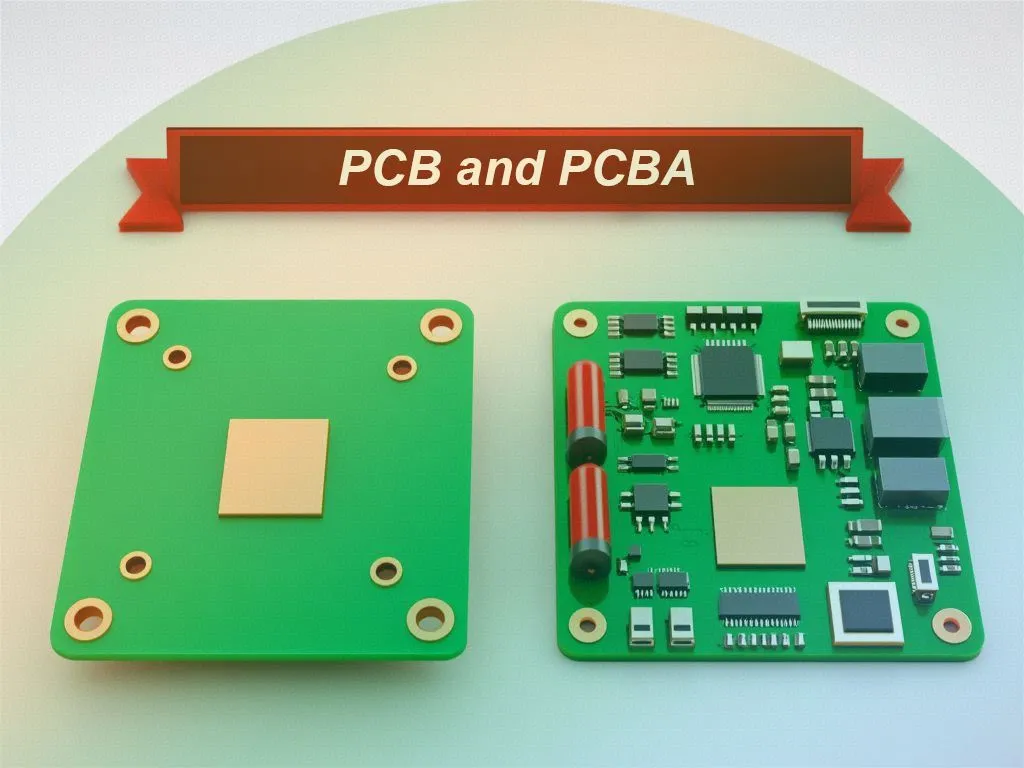
Understanding the Journey from PCB to PCBA
The process of transforming an idea into a functional electronic product starts with the PCB and ends with a fully assembled PCBA. A PCB is the foundation—a board with conductive tracks that connect electronic components. Once components are mounted and soldered onto the PCB, it becomes a PCBA, ready to power your device. Meeting technical needs at every stage ensures reliability, performance, and cost-effectiveness.
This journey involves multiple steps: designing the PCB layout, fabricating the board, preparing an accurate Bill of Material, using tools like SMT stencils for assembly, and testing the final assembly. Each phase has specific requirements that, when addressed properly, result in a high-quality product. Let’s explore these stages in detail to help you understand and meet your product’s needs.
Step 1: PCB Design – Laying the Foundation
PCB design is the first critical step in meeting your product’s technical requirements. This stage involves creating a digital blueprint of the board, defining where components will be placed and how electrical connections will be made. A well-executed PCB design minimizes errors during fabrication and assembly, ensuring your product functions as intended.
Key Technical Needs in PCB Design
- Layer Stack-Up: Determine the number of layers (e.g., single-sided, double-sided, or multi-layer) based on your circuit’s complexity. For high-speed designs, a 4-layer or 6-layer board may be necessary to manage signal integrity and reduce noise.
- Trace Width and Spacing: Calculate trace widths to handle specific current loads. For example, a trace carrying 1A might need a width of 0.5mm on a 1oz copper layer to avoid overheating. Spacing must comply with manufacturing tolerances, often 0.15mm or more, to prevent short circuits.
- Impedance Control: For high-frequency signals, maintain consistent impedance (e.g., 50 ohms for RF applications) by adjusting trace dimensions and dielectric materials.
- Component Placement: Strategically place components to minimize signal delays and interference. Keep high-speed components close to connectors to reduce trace lengths.
A robust PCB design also considers thermal management, ensuring heat dissipation through vias or copper pours. By addressing these technical needs upfront, you avoid costly redesigns later. Software tools can simulate signal behavior and identify potential issues before fabrication begins.
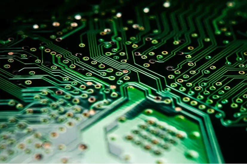
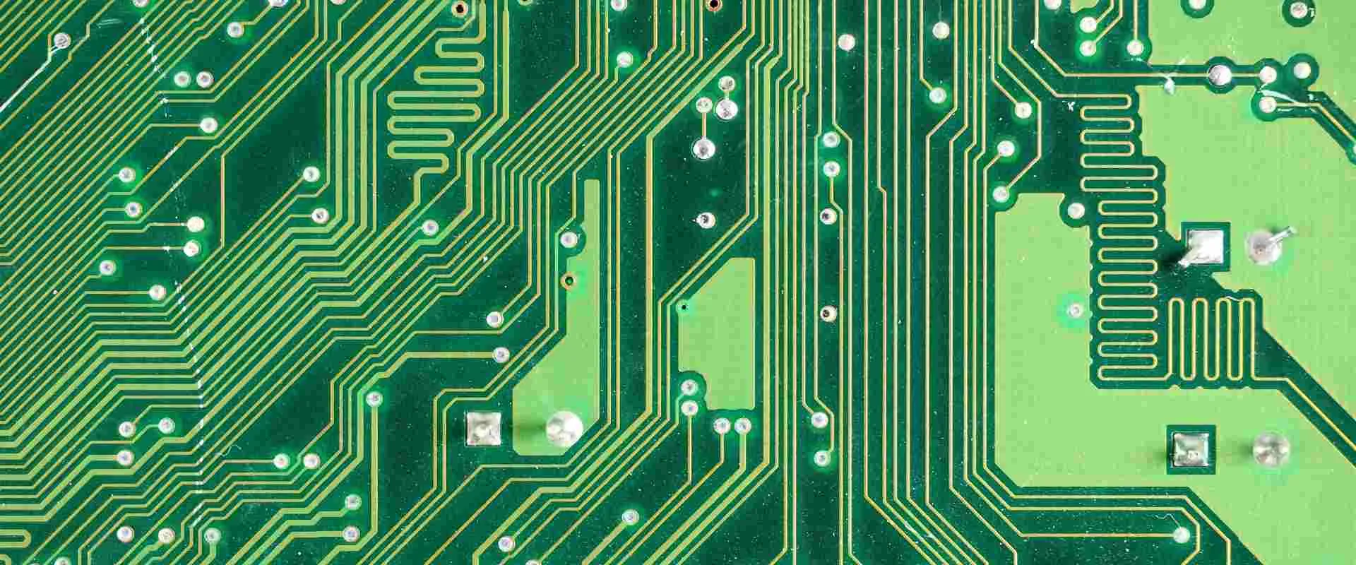
Step 2: PCB Fabrication – Turning Design into Reality
Once the design is finalized, PCB fabrication transforms your digital blueprint into a physical board. This process involves etching copper layers, drilling holes for vias and mounting, and applying protective coatings. Meeting technical requirements during PCB fabrication ensures the board can withstand assembly and operational stresses.
Technical Requirements for PCB Fabrication
- Material Selection: Choose the right substrate, such as FR-4 for standard applications or high-frequency materials like Rogers for RF designs. The dielectric constant (e.g., 4.5 for FR-4) impacts signal speed and must match design needs.
- Manufacturing Tolerances: Ensure the fabricator can meet tight tolerances, such as ±0.1mm for hole sizes or ±0.05mm for trace widths, to avoid misalignment during assembly.
- Surface Finish: Select a finish like HASL (Hot Air Solder Leveling) for cost-effectiveness or ENIG (Electroless Nickel Immersion Gold) for better solderability and corrosion resistance, especially for fine-pitch components.
- Panelization: For mass production, panelize multiple PCBs into a single sheet to optimize manufacturing efficiency, ensuring breakaway tabs or V-scoring for easy separation.
During PCB fabrication, quality control is vital. Inspections for layer alignment, copper thickness (typically 1oz or 2oz per square foot), and drill accuracy prevent defects that could affect assembly. Partnering with a reliable manufacturer ensures your boards meet these stringent requirements.
Step 3: Preparing the Bill of Material (BOM) – Ensuring Component Accuracy
A Bill of Material (BOM) is a detailed list of all components required for your PCBA. It serves as a roadmap for procurement and assembly, ensuring every part is accounted for. An accurate BOM prevents delays and errors, keeping your project on track.
Technical Needs for a Comprehensive BOM
- Component Details: Include part numbers, descriptions, quantities, and manufacturer information for every component, from resistors (e.g., 1kΩ, 1/4W) to microcontrollers.
- Footprint Matching: Verify that component footprints in the BOM match the PCB design to avoid placement issues. For instance, a 0805 resistor must correspond to an 0805 pad size on the board.
- Availability and Lead Times: Check stock availability and lead times for critical components, especially during global supply chain constraints, to avoid production delays.
- Alternatives: List substitute components with identical specifications (e.g., voltage rating, tolerance) in case primary parts are unavailable.
A well-prepared BOM streamlines the transition from PCB to PCBA by ensuring all parts are ready for assembly. Digital tools can help organize and validate your BOM, reducing the risk of mistakes.
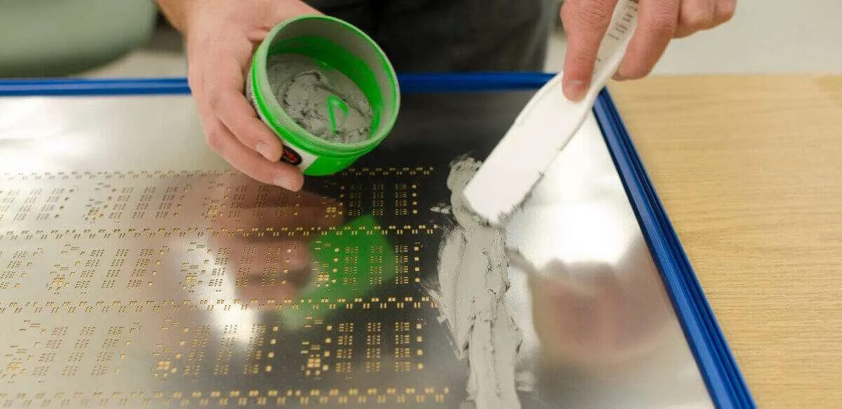
Step 4: SMT Stencil – Precision in Component Assembly
Surface Mount Technology (SMT) stencils are essential for applying solder paste accurately during PCBA. These thin metal sheets, often made of stainless steel, have openings that align with the PCB’s solder pads. Using an SMT stencil ensures precise solder placement, which is critical for small, densely packed components.
Technical Requirements for SMT Stencil Design and Use
- Aperture Design: Match stencil apertures to pad sizes, typically with a 1:1 ratio for standard components or a slight reduction (e.g., 90%) for fine-pitch parts to prevent excess solder.
- Thickness: Choose a stencil thickness based on component types. A 0.1mm to 0.15mm thickness works for most SMT components, while thicker stencils (0.2mm) suit larger parts with higher solder volume needs.
- Alignment: Ensure precise alignment with the PCB using fiducial marks or tooling holes to avoid solder paste misplacement.
- Material Durability: Opt for laser-cut stainless steel stencils for durability and precision, especially for high-volume production runs.
Proper SMT stencil usage reduces defects like solder bridges or insufficient solder joints, which can compromise the PCBA’s reliability. Regular cleaning and inspection of the stencil also maintain consistency across multiple boards.
Step 5: PCBA – Bringing It All Together
The final stage is PCBA, where components are mounted and soldered onto the fabricated PCB. This process involves both automated and manual techniques, depending on the components and production volume. Meeting technical needs during assembly ensures the board functions correctly in your final product.
Key Technical Needs in PCBA
- Solder Paste Application: Use the SMT stencil to apply solder paste evenly, followed by inspection to confirm coverage and volume. Automated optical inspection (AOI) systems can detect errors at this stage.
- Component Placement: Employ pick-and-place machines for SMT components, ensuring accuracy down to 0.01mm for fine-pitch parts like QFN packages.
- Reflow Soldering: Heat the board in a reflow oven with a controlled temperature profile (e.g., peak at 245°C for lead-free solder) to melt and solidify solder paste, creating strong joints.
- Through-Hole Assembly: For through-hole components, use wave soldering or manual soldering, ensuring leads are trimmed to avoid interference.
- Testing and Inspection: Conduct functional testing, in-circuit testing (ICT), and visual inspections to verify the PCBA meets design specifications. Check for signal integrity, power consumption, and thermal performance.
Each step in PCBA requires precision to avoid issues like cold solder joints or component misalignment. Advanced equipment and skilled technicians play a crucial role in meeting these technical requirements.
Common Challenges and How to Overcome Them
Even with careful planning, challenges can arise from PCB to PCBA. Here are some common issues and solutions:
- Design Errors: Use design rule checks (DRC) in PCB software to catch mistakes like incorrect trace spacing before fabrication.
- Component Shortages: Build flexibility into your BOM with alternative parts and maintain communication with suppliers for real-time updates.
- Assembly Defects: Invest in quality SMT stencils and automated inspection tools to reduce soldering errors.
- Signal Integrity Issues: Simulate high-speed designs during the PCB design phase to identify and mitigate noise or crosstalk, adjusting trace lengths or adding shielding as needed.
Proactive measures and collaboration with experienced manufacturing partners can address these challenges, ensuring your product meets its technical goals.
Why Technical Precision Matters from PCB to PCBA
Meeting technical needs at every stage—from PCB design and fabrication to SMT stencil application and PCBA—directly impacts your product’s performance and reliability. A single oversight, like mismatched impedance or an incomplete BOM, can lead to delays, increased costs, or product failures. By focusing on precision and adhering to industry standards, you ensure your electronic device operates as intended, whether it’s a consumer gadget or an industrial system.
At ALLPCB, we understand the importance of technical accuracy. Our expertise in PCB fabrication, design support, and assembly services helps you navigate this complex process with confidence. We provide tailored solutions to meet your specific requirements, ensuring a seamless transition from concept to completed PCBA.
Conclusion: Building Success with the Right Partner
From the initial PCB design to the final PCBA, meeting your product’s technical needs requires attention to detail, the right tools, and a deep understanding of each process. By focusing on critical aspects like PCB fabrication, SMT stencil precision, and a comprehensive Bill of Material, you set the stage for a successful product launch. Every step, when executed with care, contributes to a reliable and efficient electronic device.
Partnering with a trusted provider like ALLPCB ensures you have the support and resources to meet these requirements. Whether you’re tackling a simple prototype or a complex multi-layer design, we’re here to help you achieve your goals. Let’s work together to turn your vision into a reality with precision and expertise.


