 ALLPCB


Designing a printed circuit board (PCB) involves many critical decisions, and one of the most important is determining the correct line width, also known as trace width. If you're searching for a PCB line width calculator online or a trace width calculator, or wondering what affects PCB line width, you've come to the right place. In this comprehensive guide, we'll break down the essentials of PCB line width calculation, explain the factors that influence it, and provide actionable insights to help you design reliable and efficient circuit boards.
Whether you're a beginner or an experienced engineer, understanding trace width is key to ensuring your PCB performs optimally without overheating or signal issues. Let's dive into the basics and go beyond to explore advanced considerations for your next project.
What Is PCB Line Width and Why Does It Matter?
PCB line width refers to the width of the copper traces on a circuit board that carry electrical signals or power between components. These traces act like tiny wires, and their width directly impacts how much current they can handle, how much heat they generate, and how well they maintain signal integrity.
Getting the line width right is crucial. If a trace is too narrow, it may overheat or fail under high current loads. If it's too wide, it can waste valuable board space and increase production costs. By using a trace width calculator or understanding the principles behind line width calculation, you can strike the perfect balance for performance and efficiency.

How to Calculate PCB Line Width: The Basics
Calculating the appropriate line width for a PCB trace involves considering the current it will carry, the allowable temperature rise, and the thickness of the copper layer. The process can be simplified with online tools like a PCB line width calculator online, but understanding the underlying principles helps you make informed decisions.
The most common method for calculating trace width is based on standards like IPC-2221, which provides guidelines for PCB design. The formula considers:
- Current (I): The amount of current the trace will carry, measured in amperes (A).
- Temperature Rise (ΔT): The acceptable increase in temperature above ambient, typically 10°C to 20°C for most designs.
- Copper Thickness (t): The thickness of the copper layer, often 1 oz/ft2 (35 μm) or 2 oz/ft2 (70 μm).
- Trace Location: Whether the trace is on an external layer (exposed to air) or an internal layer (buried within the board), as this affects heat dissipation.
A simplified version of the formula for external traces, derived from IPC-2221, is:
Trace Width (mils) = (Current (A) / (k * (Temperature Rise (°C))^b))^c
Where k, b, and c are constants (typically k=0.048, b=0.44, c=0.725 for external traces). However, using a trace width calculator can save time and reduce errors, as it automates these calculations for you.
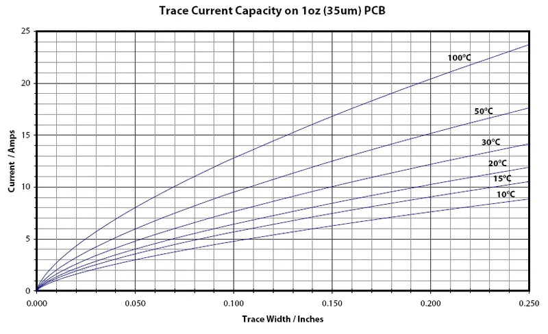
For example, if a trace needs to carry 2 A of current with a maximum temperature rise of 10°C on a 1 oz copper layer, an online calculator might suggest a width of approximately 40 mils (1 mm) for an external trace. This ensures the trace won't overheat under load.
Factors That Affect PCB Line Width
Understanding what affects PCB line width is essential for designing boards that meet performance and reliability requirements. Several key factors influence the necessary trace width for a given application:
1. Current Carrying Capacity
The primary factor in determining trace width is the amount of current the trace must carry. Higher currents require wider traces to prevent excessive heat buildup. For instance, a trace carrying 5 A will need to be significantly wider than one carrying 0.5 A under the same conditions.
2. Temperature Rise
The acceptable temperature rise dictates how much heat the trace can generate without damaging the board or nearby components. A lower temperature rise (e.g., 5°C) demands a wider trace compared to a higher rise (e.g., 20°C). Most designs aim for a 10-20°C rise to balance performance and safety.
3. Copper Thickness
Thicker copper layers can carry more current for a given trace width because they have a larger cross-sectional area. A 2 oz copper layer, for example, can handle roughly twice the current of a 1 oz layer with the same trace width and temperature rise.
4. Trace Location (Internal vs. External)
Traces on internal layers of a multilayer PCB dissipate heat less effectively than external traces because they are surrounded by insulating material. As a result, internal traces often need to be wider to handle the same current as external traces. A general rule of thumb is that internal traces may require 1.5 to 2 times the width of external traces for equivalent performance.
5. Signal Integrity and Impedance
For high-frequency or high-speed digital signals, trace width also affects impedance. A specific width is often required to match the characteristic impedance (e.g., 50 ohms for many RF applications). Incorrect trace width can lead to signal reflections and data loss, so impedance control is critical in such designs.
6. Manufacturing Constraints
The capabilities of your PCB fabrication process can limit trace width. Most standard processes can achieve trace widths as narrow as 6 mils (0.15 mm), but narrower traces may increase costs or require specialized manufacturing. Always check with your fabrication house for minimum trace width and spacing rules.
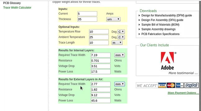
Using a PCB Line Width Calculator Online
For those new to PCB design or looking to save time, a PCB line width calculator online is an invaluable tool. These calculators are widely available and typically require you to input parameters such as:
- Current (in amperes)
- Desired temperature rise (in degrees Celsius)
- Copper thickness (in ounces per square foot or micrometers)
- Trace location (internal or external)
Once you enter these values, the calculator provides the recommended trace width in mils or millimeters. Many calculators also offer additional outputs, such as the expected voltage drop or power dissipation, which can help fine-tune your design.
Using an online tool is especially helpful when dealing with complex designs involving multiple traces with different current requirements. It ensures consistency and reduces the risk of errors compared to manual calculations.
Advanced Considerations for PCB Trace Width
Beyond the basics, several advanced factors come into play when calculating trace width for specialized applications. These considerations ensure your PCB meets the demands of high-performance or high-reliability environments.
High-Frequency Designs and Controlled Impedance
In high-frequency circuits, such as those used in RF or high-speed digital applications, trace width must be calculated to achieve a specific characteristic impedance. For example, a 50-ohm impedance is common for RF signals, and the trace width must be matched to the board's dielectric constant and layer stack-up. Online impedance calculators or simulation software can assist in determining the correct width for these scenarios.
Thermal Management
In power electronics, where traces carry high currents, thermal management becomes critical. Wider traces help dissipate heat, but you may also need to consider adding thermal vias or heat sinks to manage temperature. For instance, a trace carrying 10 A on a 1 oz copper layer might require a width of over 100 mils (2.54 mm) to keep the temperature rise below 20°C.
Space Constraints and Miniaturization
In compact designs, board space is often limited, making it challenging to use wide traces. In such cases, you might opt for thicker copper layers or multilayer boards to reduce trace width while maintaining current-carrying capacity. Balancing space constraints with electrical requirements is a common challenge in modern PCB design.
Practical Tips for PCB Line Width Design
Here are some actionable tips to help you apply line width calculations effectively in your PCB designs:
- Start with Standards: Use guidelines like IPC-2221 as a starting point for trace width calculations, especially for power traces.
- Leverage Online Tools: Take advantage of a trace width calculator to quickly estimate widths and verify manual calculations.
- Consider Worst-Case Scenarios: Design for the maximum expected current and ambient temperature to ensure reliability under all conditions.
- Account for Manufacturing Tolerances: Add a small margin (e.g., 10-15%) to calculated trace widths to accommodate variations in fabrication.
- Simulate High-Speed Designs: Use simulation software to model signal integrity and impedance for high-frequency traces.
Common Mistakes to Avoid in PCB Line Width Calculation
Even experienced designers can make errors when calculating trace widths. Here are some pitfalls to watch out for:
- Underestimating Current: Failing to account for peak currents can lead to overheating and trace failure.
- Ignoring Internal Layers: Not adjusting widths for internal traces can result in thermal issues due to poor heat dissipation.
- Neglecting Signal Integrity: Focusing only on current capacity and overlooking impedance requirements can degrade performance in high-speed designs.
- Overlooking Fabrication Limits: Designing traces narrower than the manufacturer's capabilities can lead to production issues or increased costs.
Conclusion: Mastering PCB Line Width for Better Designs
Calculating the correct line width for your PCB is a fundamental step in creating reliable, efficient, and high-performing circuit boards. By understanding the basics of trace width calculation, using tools like a PCB line width calculator online, and considering what affects PCB line width, you can design boards that meet both electrical and physical requirements.
From current capacity and temperature rise to signal integrity and manufacturing constraints, many factors influence the ideal trace width. Armed with this knowledge and practical tips, you can avoid common mistakes and optimize your designs for success. Whether you're working on a simple prototype or a complex multilayer board, mastering line width calculation will elevate the quality of your PCB projects.


