ALLPCB


In the fast-evolving world of automotive technology, Advanced Driver Assistance Systems (ADAS) are at the forefront of making vehicles safer and smarter. A critical component of these systems is the Printed Circuit Board (PCB), which must meet stringent performance and efficiency standards. So, how can we elevate ADAS PCB design to meet these demands? The answer lies in leveraging Artificial Intelligence (AI). By integrating AI into the design process, engineers can optimize layouts, improve signal integrity, and manage thermal challenges with unprecedented precision.
In this blog, we’ll dive deep into how AI transforms ADAS PCB design. From machine learning algorithms to automated layouts, we’ll explore the tools and techniques that enhance performance and efficiency. Whether you’re an engineer or a tech enthusiast, this guide will provide actionable insights into the future of automotive electronics design.
Why AI Matters in ADAS PCB Design
ADAS technologies, such as lane departure warnings, adaptive cruise control, and automatic emergency braking, rely heavily on complex electronic systems. These systems process massive amounts of data in real-time, requiring PCBs that can handle high-speed signals, maintain reliability, and operate under varying thermal conditions. Traditional PCB design methods often struggle to keep up with these demands due to time constraints and human error.
AI steps in as a game-changer. By automating repetitive tasks, predicting potential issues, and optimizing designs, AI reduces design cycles and boosts accuracy. For instance, AI-driven tools can analyze thousands of layout possibilities in minutes, a task that would take humans days or weeks. This efficiency is vital for meeting the tight deadlines of automotive projects while ensuring top-notch performance.
The Role of Machine Learning in ADAS PCB Design
Machine learning, a subset of AI, plays a pivotal role in refining PCB design for ADAS applications. Unlike traditional rule-based systems, machine learning algorithms learn from vast datasets, identifying patterns and making decisions based on past designs and simulations.
One key area where machine learning excels is in component placement. In ADAS PCBs, components like microcontrollers, sensors, and power regulators must be positioned to minimize interference and optimize signal paths. Machine learning algorithms can analyze previous designs and suggest placements that reduce electromagnetic interference (EMI) by up to 30%, based on industry studies. This leads to cleaner signals and more reliable systems.
Moreover, machine learning can predict potential design flaws before they occur. By training on historical data of PCB failures, these algorithms can flag issues like improper trace widths or insufficient spacing, which could lead to signal degradation at high frequencies (e.g., above 1 GHz, common in radar-based ADAS systems). This predictive capability saves time and reduces costly redesigns.
Automated PCB Layout: Speeding Up Design Cycles
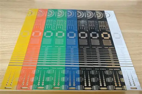
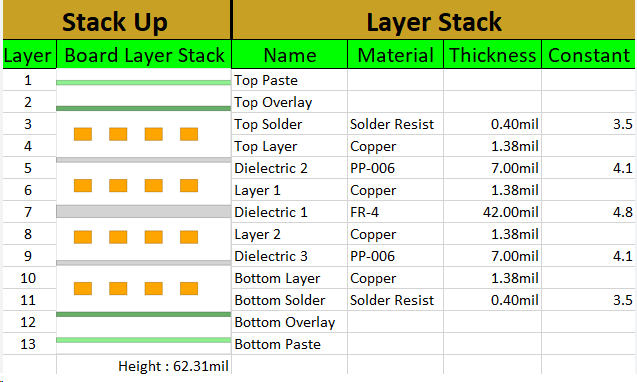
Automated PCB layout is one of the most tangible benefits of AI in ADAS design. Creating a layout manually involves balancing numerous constraints, such as trace lengths, via placements, and layer stacking. For ADAS systems, which often require multi-layer boards (8 to 16 layers or more), this process can be incredibly time-consuming.
AI-driven automation tools tackle this challenge by generating layouts based on predefined design rules and optimization goals. These tools can route traces for high-speed signals (e.g., operating at 5 Gbps for camera data) while ensuring minimal crosstalk and impedance mismatches. For example, AI can maintain a consistent impedance of 50 ohms across differential pairs, a critical factor for data integrity in ADAS communication protocols like CAN-FD or Ethernet.
The result? Design cycles that once took weeks can now be completed in days or even hours. This speed is crucial in the automotive industry, where time-to-market can determine a product’s success. Additionally, automated layouts reduce human error, ensuring that designs meet the strict safety and performance standards of ADAS applications.
AI-Driven Signal Integrity: Ensuring Reliable Data Transmission
Signal integrity is a cornerstone of ADAS PCB performance. These systems rely on high-speed data transmission between sensors, processors, and actuators. Any degradation in signal quality—due to crosstalk, reflections, or EMI—can lead to errors, delays, or even system failures. For instance, a delay of just 1 nanosecond in a radar signal could miscalculate a vehicle’s distance from an obstacle, posing a safety risk.
AI-driven signal integrity analysis uses advanced simulations to predict and mitigate these issues. By modeling the behavior of high-speed signals (e.g., at frequencies of 2.4 GHz for wireless communication modules), AI tools can recommend trace widths, spacing, and termination strategies to minimize reflections. Studies suggest that AI can improve signal integrity by up to 25% compared to traditional methods, ensuring that data transmission remains reliable even in harsh automotive environments.
Furthermore, AI can adapt designs to specific ADAS components. For example, when integrating a LiDAR sensor with a processing unit, AI tools can optimize the PCB layout to handle the sensor’s unique signal characteristics, such as pulse widths and timing requirements. This level of customization is invaluable for maintaining system accuracy.
AI Thermal Management: Keeping ADAS Systems Cool
Thermal management is another critical aspect of ADAS PCB design. Automotive electronics often operate in extreme conditions, with temperatures ranging from -40°C to 85°C or higher. Excessive heat can degrade component performance, shorten lifespan, and cause system failures. For instance, a processor overheating by just 10°C beyond its rated limit can reduce its operational life by 50%.
AI enhances thermal management by simulating heat dissipation across a PCB design. Using finite element analysis (FEA) and machine learning models, AI tools can predict hotspots and suggest solutions like optimized copper pours, thermal vias, or heat sink placements. For example, AI might recommend increasing the copper thickness in a power delivery area from 1 oz to 2 oz to improve heat dissipation, reducing temperatures by up to 15°C in critical zones.
Additionally, AI can balance thermal performance with other design constraints. In an ADAS PCB, placing a high-power component near a heat-sensitive sensor could cause issues. AI algorithms can rearrange components or adjust board layers to distribute heat evenly, ensuring that no single area exceeds safe operating temperatures. This proactive approach is essential for maintaining the reliability of safety-critical systems.
Benefits of AI in ADAS PCB Design: A Summary
Integrating AI into ADAS PCB design offers a multitude of advantages that directly impact performance and efficiency. Here’s a quick overview:
- Faster Design Cycles: Automation reduces layout and verification time from weeks to days, accelerating time-to-market.
- Improved Accuracy: Machine learning predicts and prevents design flaws, cutting down on costly iterations.
- Enhanced Signal Integrity: AI optimizes high-speed signal paths, ensuring reliable data transmission for critical ADAS functions.
- Better Thermal Management: Predictive simulations help manage heat, extending component life and system reliability.
- Cost Efficiency: By minimizing errors and redesigns, AI lowers development costs, which is crucial for competitive automotive markets.
These benefits collectively enable engineers to design PCBs that meet the rigorous demands of modern ADAS technologies while staying within budget and timeline constraints.
Challenges and Future Outlook of AI in ADAS PCB Design
While AI offers transformative potential, it’s not without challenges. One hurdle is the need for high-quality data to train machine learning models. Incomplete or inaccurate datasets can lead to suboptimal designs, underscoring the importance of robust data collection in the industry. Additionally, integrating AI tools into existing workflows may require upskilling for engineers unfamiliar with these technologies.
Looking ahead, the future of AI in ADAS PCB design is promising. Advances in generative AI could enable tools to create entirely new design architectures tailored to specific ADAS applications. Imagine a system that not only optimizes a layout but also suggests novel circuit configurations for better efficiency. Furthermore, as AI algorithms become more sophisticated, real-time design adjustments during prototyping could become a reality, further streamlining the development process.

How to Get Started with AI in ADAS PCB Design
For engineers and companies looking to adopt AI in their ADAS PCB design process, the first step is to explore available tools and platforms. Many Electronic Design Automation (EDA) software providers now offer AI-powered features for layout, simulation, and verification. Start with a pilot project to test these tools on a small-scale design, measuring metrics like design time and error rates against traditional methods.
Next, invest in training. Understanding how AI algorithms work and how to interpret their outputs is crucial for maximizing their benefits. Online courses and industry webinars can provide valuable knowledge on integrating AI into PCB workflows.
Finally, collaborate with PCB manufacturing partners who support AI-driven designs. Sharing optimized design files and simulation data ensures that the final product aligns with the AI-recommended specifications, from trace impedance to thermal performance.
Conclusion: Embracing AI for the Future of ADAS
The integration of AI in ADAS PCB design is no longer a futuristic concept—it’s a practical solution that’s reshaping the automotive electronics landscape. From machine learning algorithms that predict design flaws to automated layouts that save time, AI enhances both performance and efficiency. By addressing challenges like signal integrity and thermal management with precision, AI ensures that ADAS systems remain reliable and safe under all conditions.
As the automotive industry continues to push boundaries, adopting AI-driven design tools will be essential for staying competitive. The result is not just better PCBs, but safer, smarter vehicles that transform the way we drive. So, take the leap into AI-powered design today, and unlock the full potential of your ADAS projects with cutting-edge technology.