 ALLPCB


Damaged PCB traces can bring your electronic projects to a halt, but the good news is that with the right tools and techniques, you can often repair them yourself. Whether you're dealing with a simple circuit board or a more complex design, fixing damaged PCB traces is a valuable skill that can save time and money. In this step-by-step guide, we'll walk you through the process of repairing damaged PCB traces, ensuring your board functions as good as new. From identifying the issue to testing the repair, we’ve got you covered with clear, actionable steps for PCB traces repair.
Understanding PCB Traces and Why They Get Damaged
Printed Circuit Boards (PCBs) are the foundation of most electronic devices. They consist of thin copper pathways, known as traces, that connect components and allow electrical signals to flow. These traces are delicate, often as thin as 0.1 mm, and can be damaged due to various reasons like physical stress, overheating, or corrosion. When a trace is broken or damaged, it disrupts the electrical flow, causing the device to malfunction or stop working entirely.
Common causes of damaged PCB traces include:
- Physical Damage: Dropping a device or applying too much force during assembly can crack or break traces.
- Overheating: Excessive heat from soldering or high current can burn or melt traces, especially if the current exceeds the trace’s capacity (e.g., a trace designed for 1A carrying 2A).
- Corrosion: Exposure to moisture or chemicals can erode copper traces over time, leading to breaks.
- Manufacturing Defects: Poor design or low-quality materials can make traces prone to damage during use.
Understanding the cause of the damage can help prevent future issues, but for now, let’s focus on the steps to repair a simple circuit board with damaged traces.
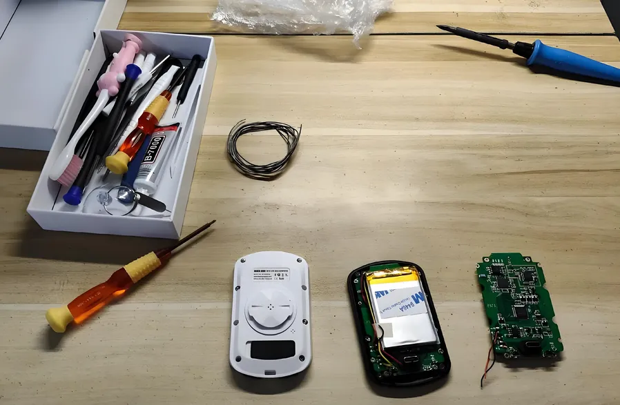
Tools and Materials Needed for PCB Trace Repair
Before starting the repair process, gather the necessary tools and materials. Having everything ready ensures a smoother workflow and reduces the risk of further damage to your simple circuit board. Here’s what you’ll need:
- Soldering Iron: A fine-tip soldering iron (15-30W) for precise work on small traces.
- Solder: Use rosin-core solder with a diameter of 0.5-1.0 mm for electronics.
- Desoldering Braid or Pump: To remove old solder if needed.
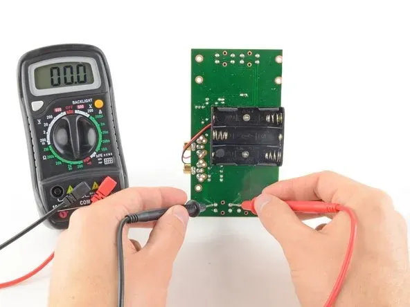
- Multimeter: For testing continuity and identifying breaks in traces.
- Utility Knife or X-Acto Knife: To scrape away solder mask and expose copper.
- Fine-Gauge Wire: For creating jumper connections if a trace cannot be directly repaired (e.g., 30 AWG wire).
- Isopropyl Alcohol (IPA): At least 90% concentration for cleaning the board.
- Cotton Swabs or Brush: For applying IPA and cleaning debris.
- Magnifying Glass or Microscope: To inspect small traces and ensure precision.
- Solder Mask or Epoxy (Optional): To protect repaired areas after fixing.
- Tweezers: For handling small components or wires.
With these tools in hand, you’re ready to tackle the repair of damaged PCB traces. Make sure to work in a well-lit, static-free environment to avoid additional damage.
Related Reading: PCB Trace Repair for Beginners: A Hobbyist's Guide to Saving Damaged Boards
Step-by-Step Guide to Repair Damaged PCB Traces
Repairing damaged PCB traces may seem intimidating, but by following these steps for PCB traces repair, even beginners can achieve reliable results on a simple circuit board. Let’s break it down into manageable steps.
Step 1: Inspect and Identify the Damaged Trace
Start by visually inspecting the PCB under good lighting. Use a magnifying glass or microscope to spot breaks, burns, or corrosion in the copper traces. Damaged areas may appear as thin gaps, darkened spots, or completely severed lines. If the damage isn’t obvious, use a multimeter set to continuity mode to test the trace. Place the probes on either end of a suspected trace; if there’s no beep or reading, the trace is broken.
Tip: Traces are often covered by a green solder mask. If you suspect damage beneath the mask, gently scrape it away with a utility knife to expose the copper for testing.
Step 2: Clean the Damaged Area
Once you’ve located the damaged trace, clean the area to remove dirt, debris, or old solder. Dip a cotton swab or small brush in isopropyl alcohol and gently scrub the area. This step ensures better adhesion for soldering and prevents contamination during repair. Dry the area completely with a lint-free cloth or compressed air before proceeding.
Caution: Avoid excessive force while cleaning to prevent further damage to nearby traces or components.
Step 3: Expose the Copper Trace (If Necessary)
If the damaged trace is covered by solder mask, use a utility knife or fine sandpaper to carefully scrape away the mask and expose the bare copper. Work slowly to avoid cutting into the copper or damaging adjacent traces. You only need to expose a small section on either side of the break—about 2-3 mm is usually enough for soldering.
Step 4: Assess the Extent of Damage
Determine if the trace can be repaired by soldering directly or if a jumper wire is needed. For small breaks (less than 5 mm), soldering may suffice. For larger gaps or completely severed traces, a jumper wire will be necessary to bridge the connection. If the trace is burnt or corroded over a wide area, consider replacing the section with wire to ensure reliable conductivity.
Step 5: Repair Small Breaks with Solder
For minor breaks, apply a small amount of solder to bridge the gap. Heat your soldering iron to around 300°C (572°F) and tin the tip with a thin layer of solder. Then, touch the tip to one side of the broken trace, adding a small bead of solder. Repeat on the other side, allowing the solder to flow across the gap and form a connection. Be precise—excess solder can create shorts with nearby traces.
After soldering, inspect the joint with a magnifying glass to ensure it’s smooth and there are no cold solder joints (dull or cracked appearance). Use a multimeter to confirm continuity across the repaired trace.
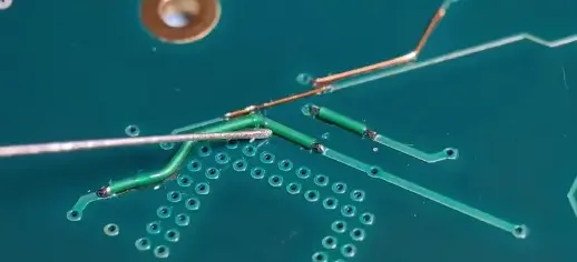
Step 6: Use a Jumper Wire for Larger Breaks
If the break is too large to solder directly, cut a piece of fine-gauge wire (e.g., 30 AWG) to span the gap. Strip a small amount of insulation from both ends of the wire. Tin the exposed ends with solder, then solder one end to the trace on one side of the break and the other end to the trace on the opposite side. Route the wire neatly to avoid interference with other components, and secure it with a dab of hot glue or epoxy if needed.
Tip: For boards with high-frequency signals (above 100 MHz), keep jumper wires as short as possible to minimize impedance changes, which can affect signal integrity. A typical trace might have an impedance of 50 ohms, and a long jumper can introduce unwanted noise or delay.
Step 7: Protect the Repaired Area
After repairing the trace, apply a layer of solder mask or epoxy over the exposed copper to protect it from corrosion and physical damage. Use a small brush or applicator to apply the coating, and allow it to cure as per the manufacturer’s instructions. This step is optional but recommended for long-term reliability, especially in humid environments.
Step 8: Test the PCB for Functionality
Once the repair is complete, test the PCB to ensure it works correctly. Reassemble any removed components, power up the board, and check for proper operation. Use a multimeter to verify voltage levels at key points (e.g., 5V or 3.3V as per the circuit design) and ensure there are no shorts or open circuits. If the board doesn’t function as expected, recheck your repair for issues like poor solder joints or incorrect wiring.
Related Reading: The Ultimate Guide to PCB Trace Repair: Step by Step for Engineers
Tips for Preventing Future PCB Trace Damage
Repairing damaged PCB traces is a great skill, but preventing damage in the first place is even better. Here are some practical tips to protect your simple circuit board:
- Handle with Care: Always handle PCBs gently to avoid physical stress or accidental drops.
- Use Proper Soldering Techniques: Avoid overheating traces by limiting soldering iron contact to 2-3 seconds per joint.
- Protect Against Moisture: Store PCBs in dry, static-free environments, and consider conformal coating for boards exposed to humidity.
- Design for Durability: When designing or ordering PCBs, ensure trace widths are adequate for the expected current (e.g., use a trace width calculator to avoid undersizing traces for high-current applications).
Common Challenges in PCB Trace Repair and How to Overcome Them
Repairing damaged PCB traces can come with hurdles, especially for beginners working on a simple circuit board. Here are some common issues and solutions:
- Trace Too Small to Solder: If the trace is too narrow for direct soldering, use a jumper wire instead. Practice on scrap boards to improve precision with fine-tip soldering irons.
- Accidental Shorts: If solder bridges to nearby traces, use desoldering braid to remove excess solder. Double-check with a multimeter to ensure no shorts remain.
- Damaged Pads: If the solder pad near a trace is damaged, scrape away the mask to expose more copper and solder directly to the trace, or use a jumper wire to bypass the pad.
- Signal Integrity Issues: For high-speed circuits, long jumper wires can introduce delays (e.g., a 10 cm wire can add up to 0.5 ns delay). Keep wires short and route them close to the original trace path.
When to Seek Professional Help for PCB Repairs
While many damaged PCB traces can be fixed at home, some situations call for professional assistance. If the board has multiple layers (more than 2), extensive damage, or critical high-frequency signals (above 1 GHz), DIY repairs may not be feasible without specialized equipment like X-ray inspection tools. Additionally, if the board is part of a high-value or safety-critical device, it’s safer to consult a professional repair service to avoid costly mistakes.
Conclusion: Restoring Functionality to Your PCB
Repairing damaged PCB traces on a simple circuit board is a practical skill that can breathe new life into malfunctioning electronics. By following the steps for PCB traces repair outlined in this guide—inspecting the damage, cleaning the area, soldering or using jumper wires, and testing the board—you can achieve reliable results with basic tools. Remember to work patiently and precisely to avoid further damage, and take preventive measures to protect your boards in the future.
With practice, you’ll gain confidence in handling damaged PCB traces and tackling more complex repairs. Whether you’re a hobbyist or a professional, mastering these steps for PCB traces repair ensures your projects stay on track without the need for costly replacements. Keep your tools ready, and don’t let a broken trace stop your progress!


