ALLPCB


In the world of printed circuit board (PCB) design, every detail counts. One critical factor that often gets overlooked is the core thickness of the PCB substrate. So, how does core thickness impact PCB signal integrity and overall performance? Simply put, the thickness of the core, along with the properties of the substrate material, directly affects impedance, signal loss, and the ability to handle high-speed signals without reflections or distortion. In this blog, we'll dive deep into the relationship between core thickness, substrate materials, and key performance metrics like dielectric constant and signal loss, especially for high-speed PCB design.
Whether you're an engineer working on cutting-edge electronics or a hobbyist looking to optimize your next project, understanding these factors can make or break your design. Let’s explore how core thickness impedance and PCB substrate materials play a vital role in achieving top-notch PCB performance and minimizing PCB signal reflections.
What Is PCB Core Thickness and Why Does It Matter?
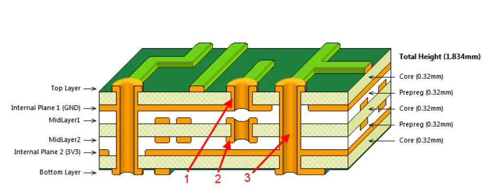
PCB core thickness refers to the thickness of the central insulating layer in a multilayer PCB, which is typically made of a substrate material like FR-4 or other advanced laminates. This core sits between conductive copper layers and plays a crucial role in the board's mechanical stability and electrical performance. Core thickness can range from as thin as 0.1 mm in flexible or high-density designs to over 1.6 mm in standard rigid boards.
Why does this matter for PCB signal integrity? The thickness of the core influences the spacing between signal traces and ground planes, which in turn affects the characteristic impedance of the traces. Impedance mismatches can lead to signal reflections, causing data errors in high-speed PCB design. Additionally, core thickness impacts how signals propagate through the board, contributing to potential signal loss if not optimized.
The Role of PCB Substrate Materials in Signal Integrity
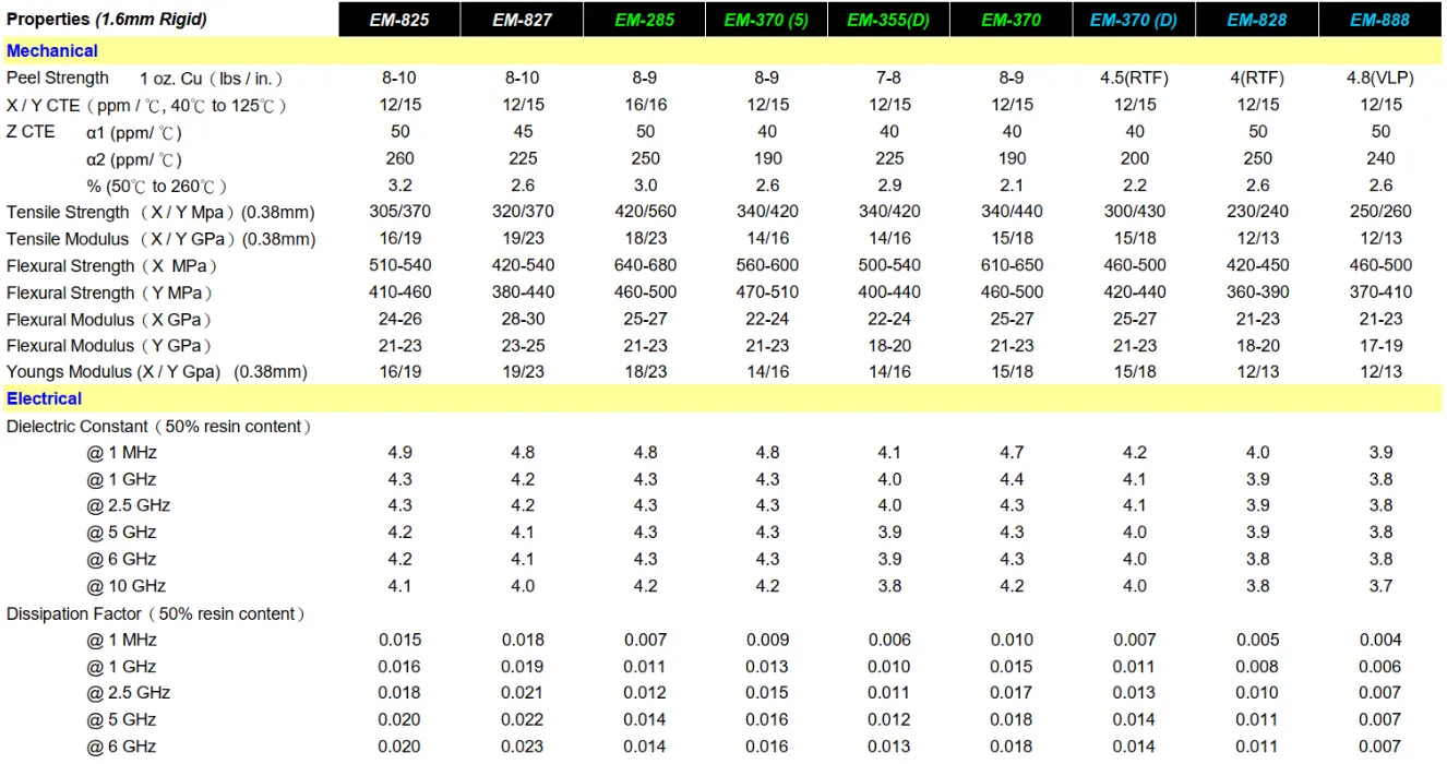
The choice of PCB substrate materials is just as important as core thickness when it comes to PCB performance. Substrate materials determine the board’s electrical properties, including the dielectric constant (Dk) and dissipation factor (Df), which directly affect signal speed and loss.
Common substrate materials include:
- FR-4: A widely used material with a dielectric constant of around 4.4–4.8. It’s cost-effective but can introduce higher signal loss at frequencies above 1 GHz.
- High-Frequency Laminates: Materials with lower Dk values (2.5–3.0) are designed for high-speed PCB design. They reduce signal distortion and loss, making them ideal for applications like 5G or RF circuits.
- Polyimide: Often used in flexible PCBs, offering good thermal stability but with varying dielectric properties depending on the specific formulation.
The dielectric constant of the substrate affects how fast signals travel through the board. A higher Dk slows down the signal, which can cause timing issues in high-speed designs. Meanwhile, the dissipation factor influences signal loss—a higher Df means more energy is lost as heat, degrading signal quality.
For example, in a design operating at 10 GHz, using a substrate with a Dk of 3.0 instead of 4.5 can increase signal speed by approximately 20%, significantly improving performance and reducing the risk of PCB signal reflections.
Core Thickness and Impedance: A Critical Relationship
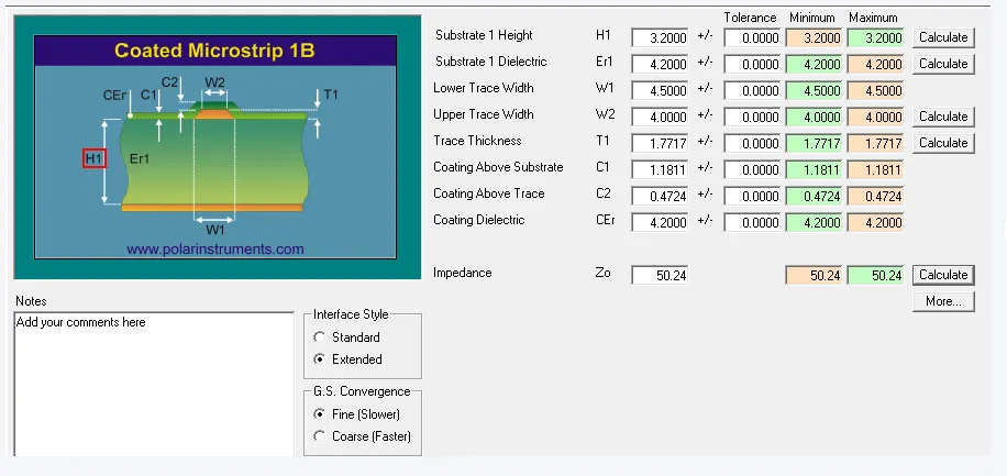
One of the most direct ways core thickness impacts PCB signal integrity is through its effect on core thickness impedance. Characteristic impedance is the resistance a signal encounters as it travels along a trace, and it must be matched to the source and load to prevent reflections.
In a typical PCB, impedance is determined by the width of the trace, the thickness of the dielectric (core or prepreg layer), and the dielectric constant of the substrate. For a microstrip trace (a trace on the outer layer over a ground plane), reducing the core thickness brings the trace closer to the ground plane, lowering the impedance. For instance, a core thickness of 0.2 mm might result in an impedance of 50 ohms for a specific trace width, while increasing the thickness to 0.4 mm could raise the impedance to 75 ohms if other factors remain constant.
Impedance mismatches caused by improper core thickness can lead to PCB signal reflections, where part of the signal bounces back along the trace, interfering with the original signal. This is especially problematic in high-speed PCB design, where even small mismatches can cause significant data errors.
To avoid this, designers often use simulation tools to calculate the ideal core thickness and trace dimensions for a target impedance, ensuring consistent signal transmission across the board.
Signal Loss and Core Thickness: Minimizing Attenuation
Another critical factor influenced by core thickness and substrate choice is signal loss, or attenuation. Signal loss occurs when a signal’s amplitude decreases as it travels through the PCB, often due to dielectric losses or conductor resistance.
Thicker cores can increase signal loss in high-frequency designs because the signal must travel through more dielectric material, which absorbs energy. For example, at 5 GHz, a signal traveling through a 1.6 mm thick FR-4 core might experience a loss of 0.5 dB per inch, whereas a thinner 0.8 mm core could reduce this loss by 20-30%, depending on other design factors.
Choosing a substrate with a low dissipation factor can also help. High-frequency laminates with Df values below 0.005 are often preferred over standard FR-4 (Df around 0.02) to minimize energy loss, especially in applications requiring long trace lengths or high data rates.
By carefully selecting core thickness and substrate material, designers can significantly reduce signal loss, ensuring reliable performance in demanding applications.
High-Speed PCB Design: Challenges and Solutions
In high-speed PCB design, where signals operate at gigabit speeds or higher, the challenges related to core thickness and substrate properties become even more pronounced. Data rates above 10 Gbps are common in modern applications like telecommunications, automotive radar, and data centers, and maintaining PCB signal integrity at these speeds requires precise control over every design element.
One major challenge is managing signal propagation delay, which is influenced by the dielectric constant of the substrate. A mismatch in propagation delay between differential pairs (common in high-speed designs) can cause skew, leading to data corruption. Using a substrate with a consistent Dk and optimizing core thickness helps minimize this issue.
Another concern is crosstalk, where signals on adjacent traces interfere with each other. Thicker cores can reduce crosstalk by increasing the separation between layers, but this must be balanced against the potential for increased signal loss.
Solutions for high-speed designs include:
- Using thinner cores for shorter signal paths and lower impedance.
- Selecting advanced substrates with stable dielectric properties across a wide frequency range.
- Implementing ground planes and vias strategically to shield signals and maintain impedance.
By addressing these factors, designers can achieve reliable PCB performance even at the highest speeds.
Practical Tips for Optimizing Core Thickness and Substrate Choice
Now that we’ve covered the technical aspects, here are some practical tips for optimizing core thickness and substrate materials to enhance PCB signal integrity and performance:
- Match Core Thickness to Application: For high-speed designs, consider thinner cores (0.1-0.2 mm) to maintain low impedance and reduce signal loss. For power electronics, thicker cores (1.6 mm or more) provide better mechanical strength.
- Choose the Right Substrate: Evaluate the frequency range of your design. Standard materials work well below 1 GHz, but for higher frequencies, invest in low-Dk, low-Df substrates.
- Simulate Before Building: Use PCB design software to simulate impedance and signal behavior with different core thicknesses and materials. This helps catch issues before manufacturing.
- Control Manufacturing Tolerances: Work with your PCB fabricator to ensure tight control over core thickness and dielectric properties, as variations can impact performance.
- Test and Iterate: Build prototypes and test for signal loss and reflections under real-world conditions to fine-tune your design.
Following these steps can help you avoid common pitfalls and achieve a design that meets both electrical and mechanical requirements.
Conclusion: Balancing Core Thickness and Substrate for Optimal Performance
The relationship between core thickness, PCB substrate materials, and PCB signal integrity is a cornerstone of effective PCB design. Core thickness directly impacts core thickness impedance, signal propagation, and the risk of PCB signal reflections, while substrate properties like dielectric constant and dissipation factor play a major role in signal loss and overall PCB performance.
For high-speed PCB design, where precision is non-negotiable, optimizing these factors can mean the difference between a flawless product and one plagued by errors. By understanding how core thickness and substrate choices affect signal behavior, and by applying practical design strategies, engineers can create boards that deliver reliable performance across a wide range of applications.
At ALLPCB, we’re committed to supporting your design journey with high-quality manufacturing and expert guidance. Whether you’re tackling a complex high-speed project or a simple prototype, paying attention to core thickness and substrate materials is a step toward success.