ALLPCB


Introduction
In the world of printed circuit boards (PCBs), 'gold fingers' might sound like a luxury feature, but they're a critical component for ensuring reliable electrical connections. These gold-plated edge connectors are found on everything from computer memory modules to industrial control systems, offering unmatched conductivity and durability. For engineers designing high-performance electronics, understanding the applications and manufacturing standards of gold fingers is essential to creating robust, long-lasting devices. In this blog, we'll dive into what gold fingers are, how they're used, and the precise standards that govern their production—giving you the insights you need to optimize your next PCB project.
Gold fingers stand out because of their ability to withstand repeated insertions, resist corrosion, and maintain signal integrity, making them indispensable in modern electronics. Whether you're troubleshooting a design or specifying requirements for a new board, this guide will equip you with practical knowledge straight from the industry trenches. Let's explore the fascinating role of gold fingers in PCBs and the rigorous processes behind their creation.
What Are Gold Fingers in PCBs?
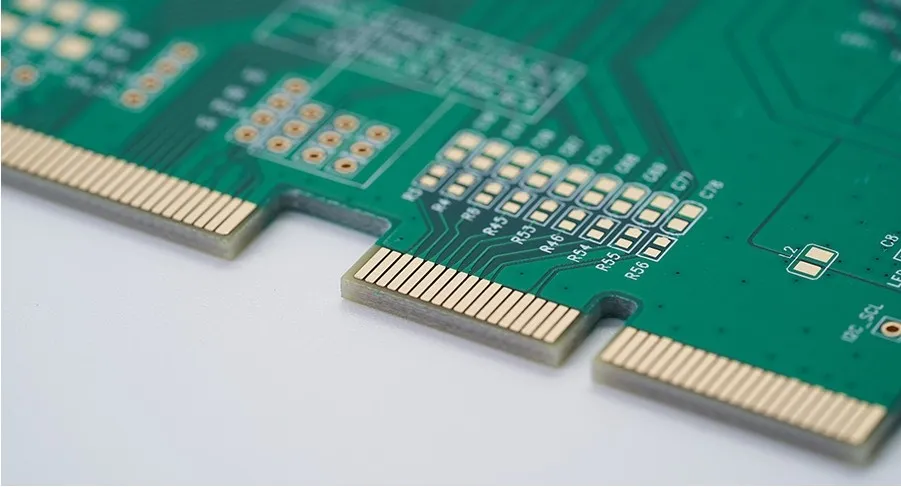
Gold fingers are the gold-plated connectors along the edge of a PCB, designed to plug into a corresponding slot or socket. Named for their finger-like appearance, these connectors are typically made by electroplating a thin layer of gold over a nickel undercoat on copper pads. The gold layer—often ranging from 2 to 50 microinches (0.05 to 1.27 micrometers)—provides excellent conductivity and resistance to wear, while the nickel acts as a barrier to prevent diffusion between the copper and gold.
These connectors are a staple in devices requiring frequent connections, like RAM sticks, graphics cards, and USB drives. Their golden hue isn't just for show; gold's low contact resistance (around 20-50 milliohms) and immunity to oxidation ensure stable performance over thousands of insertion cycles. For engineers, this means gold fingers are a go-to solution when reliability is non-negotiable.
Key Applications of Gold Fingers in PCBs
Gold fingers shine in applications where durability and signal quality are paramount. Here's a breakdown of their most common uses:
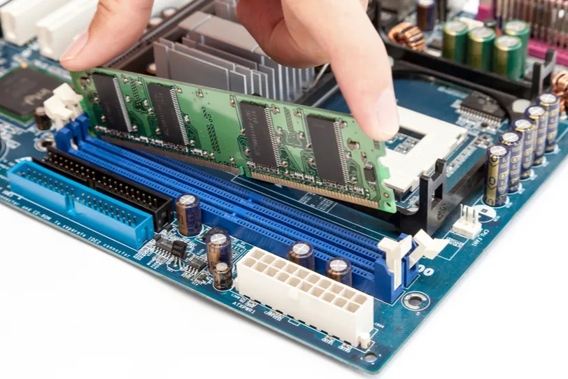
1. Computer Peripherals and Memory Modules
In PCs, gold fingers connect memory modules (like DDR5 RAM) and expansion cards (like GPUs) to the motherboard. With insertion cycles often exceeding 100 and signal speeds surpassing 3 GHz, gold's low resistance and corrosion resistance keep data flowing smoothly. For instance, a typical DDR4 DIMM might use 30 microinches of gold to handle 2,400 MT/s transfer rates without degradation.
2. Industrial and Automotive Systems
Industrial controllers and automotive ECUs rely on gold fingers for rugged, long-term performance. In harsh environments—think temperatures from -40°C to 85°C or high-vibration settings—gold prevents signal loss and connector wear. An automotive airbag controller, for example, might use gold fingers to ensure a 15-year lifespan with zero failures.
3. Consumer Electronics
From smartphones to game consoles, gold fingers link internal boards or connect external accessories. Their ability to maintain signal integrity at high frequencies (e.g., 5G signals at 3.5 GHz) makes them ideal for compact, high-speed devices. A USB-C adapter board might use 5 microinches of gold for cost efficiency while still meeting performance specs.
4. Networking Equipment
Routers and servers use gold fingers in backplanes and daughter cards to handle high-speed data—often exceeding 10 Gbps. Here, impedance control (typically 50 ohms) and minimal signal attenuation are critical, and gold's conductivity ensures these specs are met consistently.
Why Gold? The Science Behind the Choice
Why not use cheaper metals like copper or silver? The answer lies in gold's unique properties. Copper, while highly conductive (5.96 × 10? S/m), oxidizes quickly, raising contact resistance over time. Silver offers great conductivity (6.30 × 10? S/m) but tarnishes in humid or sulfur-rich environments, compromising reliability. Gold, with a conductivity of 4.11 × 10? S/m, resists corrosion and maintains stable contact resistance—crucial for applications with 10,000+ mating cycles.
To boost durability, gold is often alloyed with 5-10% cobalt or nickel during plating, creating 'hard gold' that withstands abrasive wear. This combo delivers a hardness of 130-200 Vickers, far tougher than pure gold's 25 Vickers. For engineers, this means gold fingers can handle the mechanical stress of repeated insertions without cracking or peeling.
Manufacturing Standards for Gold Fingers
Producing gold fingers isn't a free-for-all; it's governed by strict industry standards to ensure performance and compatibility. Let's unpack the key guidelines and processes.
Industry Standards: IPC and Beyond
The Association Connecting Electronics Industries (IPC) sets the gold standard—pun intended—for PCB manufacturing. Key specs include:
- IPC-6012: Defines performance criteria for rigid PCBs, mandating gold thickness between 2 and 50 microinches for edge connectors, depending on the class (e.g., Class 2 for commercial, Class 3 for aerospace).
- IPC-4552: Focuses on electroless nickel immersion gold (ENIG), but its principles apply to gold finger plating. It recommends 3-6 microinches of gold over 120-240 microinches of nickel for corrosion resistance.
- IPC-A-600: Provides visual acceptance criteria, ensuring gold fingers are free of defects like pitting or uneven plating.
Military standards like MIL-G-45204 may push gold thickness to 50 microinches for extreme reliability, but most commercial applications stick to 10-30 microinches to balance cost and performance.
The Manufacturing Process
Creating gold fingers involves precision at every step:
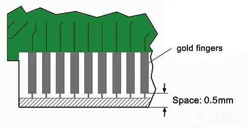
1. Base Preparation: Copper pads are etched along the PCB edge, typically 0.031 to 0.125 inches wide, per IPC tolerances.
2. Nickel Plating: A 100-200 microinch nickel layer is electroplated over the copper to prevent diffusion and add strength.
3. Gold Plating: Hard gold (alloyed with cobalt or nickel) is electroplated to the specified thickness. For high-density boards, selective plating keeps costs down by targeting only the fingers.
4. Beveling: Edges are beveled at 20-45° to ease insertion into slots, reducing wear on both the PCB and connector.
5. Quality Control: Automated optical inspection (AOI) and resistance testing (aiming for <50 milliohms) verify plating uniformity and conductivity.
Design Constraints
Engineers must follow specific layout rules:
- Spacing: Keep plated-through holes (PTH) at least 1 mm from gold fingers to avoid shorting during beveling.
- Copper-Free Inner Layers: Inner layers near the edge must lack copper to prevent exposure after cutting.
- Length Limits: Gold finger pads shouldn't exceed 40 mm to maintain structural integrity.
Deviating from these can lead to weak boards or signal issues, like impedance mismatches that disrupt high-speed data.
Challenges in Gold Finger Manufacturing
Even with standards, challenges arise:
- Cost: Gold's price (around $80/gram in 2025) makes thick plating expensive. Thin layers (e.g., 5 microinches) cut costs but may wear out faster.
- Plating Uniformity: Uneven gold thickness can cause contact failures. Advanced plating machines with ±10% tolerance help, but precision is key.
- Wear Over Time: High-insertion applications (e.g., 50,000 cycles) can erode even hard gold, requiring thicker plating or alternative materials like beryllium copper.
For engineers, balancing these factors means weighing reliability against budget—a classic design trade-off.
How ALLPCB Supports Gold Finger Projects
When it comes to bringing gold finger designs to life, partnering with a capable manufacturer is crucial. ALLPCB offers quick-turn prototyping and advanced manufacturing that cater to engineers' needs. With capabilities like precise gold plating up to 50 microinches and global logistics ensuring fast delivery, we help you meet tight deadlines without sacrificing quality. Our expertise in high-density interconnects (HDI) and impedance-controlled boards ensures your gold fingers perform flawlessly, whether for a 10 Gbps server or a rugged automotive ECU. For projects demanding reliability and speed, ALLPCB's end-to-end solutions have you covered.
Conclusion
Gold fingers are more than a shiny detail—they're a cornerstone of reliable PCB design, bridging the gap between boards and their sockets with unmatched performance. From powering your laptop's RAM to keeping industrial systems humming, their applications are vast and vital. By adhering to manufacturing standards like IPC-6012 and mastering the plating process, engineers can ensure these connectors stand the test of time. Next time you're speccing out a PCB, consider how gold fingers can elevate your design—and how precision manufacturing makes it all possible.
Got a project in mind? Understanding gold fingers is your first step to building electronics that last. Dive into the specs, tweak your layout, and watch your design shine—literally and figuratively.