 ALLPCB


Digital signage has become a cornerstone of modern advertising, powering everything from retail displays to outdoor billboards. At the heart of these systems lies the printed circuit board (PCB), a critical component that drives functionality. If you're looking to understand or replicate existing designs, digital signage PCB reverse engineering offers a pathway to analyze and learn from these intricate layouts. This process involves dissecting a PCB to uncover its design secrets, from schematics to component placement, enabling you to create similar or improved solutions for advertising displays.
In this comprehensive guide, we'll dive deep into the world of analyzing display PCB designs, understanding PCB layouts for advertising, and reverse engineering PCB schematics. Whether you're an engineer, designer, or business owner in the digital signage industry, this blog will provide actionable insights into learning from existing PCB designs to enhance your projects. Let’s explore the techniques, tools, and best practices to master this process.
What is Digital Signage PCB Reverse Engineering?
Reverse engineering a PCB in the context of digital signage means taking apart an existing board to study its design and functionality. This process helps you understand how the circuitry works, the components used, and the layout strategies employed to meet the demands of high-performance displays. By doing so, you can replicate or improve upon designs for applications like LED screens, LCD monitors, or interactive kiosks used in advertising.
The goal of digital signage PCB reverse engineering isn't just to copy a design but to gain insights into the engineering choices behind it. For instance, you might discover how a board handles high-speed signals for video output or manages power distribution for bright LED arrays. This knowledge can inspire innovative solutions tailored to your specific needs in the advertising sector.
Why Reverse Engineer Digital Signage PCBs?
There are several reasons why engineers and companies turn to reverse engineering for digital signage PCBs:
- Cost Efficiency: Creating a new design from scratch can be expensive. Reverse engineering allows you to build on proven designs, saving time and resources.
- Legacy Support: If a signage system is outdated and replacement parts are unavailable, reverse engineering helps recreate or repair the PCB.
- Competitive Analysis: Understanding how leading designs function can provide insights into industry standards and innovations.
- Customization: By studying existing layouts, you can modify designs to better suit specific advertising applications, such as adding new features or optimizing power usage.
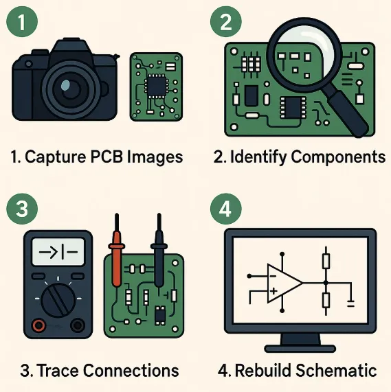
Key Steps in Analyzing Display PCB Designs
To successfully reverse engineer a digital signage PCB, you need a systematic approach. Below are the essential steps to guide you through analyzing display PCB designs and extracting valuable information.
1. Gather the Right Tools and Equipment
Before starting, ensure you have the necessary tools to safely and accurately analyze the PCB. Common tools include:
- Multimeter: For measuring voltage, resistance, and continuity to understand electrical paths.
- Microscope or Magnifying Glass: To inspect tiny components and traces on the board.
- X-Ray Imaging: Useful for multilayer boards to see internal layers without damaging the PCB.
- Schematic Capture Software: To recreate the circuit diagram based on your findings.
- Desoldering Tools: To remove components for closer inspection without causing damage.
Having the right tools ensures precision while working on delicate signage boards that often handle high-speed data (e.g., HDMI signals at 1.65 Gbps for full HD video output) and complex power requirements.
2. Document the Physical Layout
Start by photographing the PCB from multiple angles to capture every detail. Note the placement of major components like microcontrollers, power regulators, and connectors. Digital signage PCBs often have specific layouts to minimize signal interference, especially for high-frequency video signals. For example, you might notice that traces for data lines are kept short and routed away from power lines to reduce electromagnetic interference (EMI).
Measure the board dimensions and create a rough sketch of the layout. Pay attention to the layer stack-up if it's a multilayer board, as many signage PCBs use 4 to 8 layers to accommodate complex routing.

3. Identify and Catalog Components
Next, identify each component on the board. Look for markings or part numbers on ICs, resistors, capacitors, and other elements. Use datasheets to understand their specifications, such as a voltage regulator handling 5V output for LED drivers or a capacitor rated at 100uF for smoothing power supply ripples.
Create a bill of materials (BOM) listing each component, its role, and its placement on the board. This step is crucial for understanding PCB layouts for advertising because component selection often reflects design priorities, like power efficiency for outdoor displays exposed to varying temperatures.
4. Trace the Circuit Paths
Tracing the connections between components is the core of reverse engineering PCB schematics. Use a multimeter to check continuity between points and map out how signals and power flow through the board. For digital signage, pay special attention to:
- Power Distribution: How voltage (e.g., 12V or 24V for LED panels) is managed across the board.
- Signal Integrity: How data lines for video or control signals are routed to avoid crosstalk or delays.
- Ground Planes: Often used in signage PCBs to reduce noise and stabilize performance.
This step can be time-consuming, especially for multilayer boards where traces are hidden between layers. In such cases, X-ray imaging or careful desoldering may be necessary.
5. Reconstruct the Schematic
Using the data you've collected, recreate the schematic diagram with software tools designed for PCB design. This visual representation shows how components are electrically connected, offering a clear picture of the board's functionality. For instance, you might find that a signage PCB uses a specific microcontroller to process video input at 1080p resolution, paired with a driver circuit delivering 500mA per LED channel.
Reconstructing the schematic is a vital part of learning from existing PCB designs, as it allows you to see the design logic behind the hardware.
Challenges in Reverse Engineering Digital Signage PCBs
While reverse engineering offers many benefits, it comes with challenges that require careful handling, especially for complex digital signage systems.
Multilayer Complexity
Most digital signage PCBs are multilayered to support compact designs with high-density components. Without access to internal layers, tracing connections becomes difficult. Techniques like X-ray imaging can help, but they require specialized equipment and expertise.
Proprietary Components
Some signage boards use custom or proprietary chips with no public datasheets. In such cases, you may need to infer their function based on surrounding circuitry or behavior during operation, which can be imprecise.
Signal Integrity Issues
High-speed signals in digital signage, such as those for 4K video output at frequencies above 3 GHz, are sensitive to impedance mismatches. Reverse engineering must account for trace widths (often 6-8 mils for controlled impedance) and dielectric materials to ensure the replicated design maintains performance.
Best Practices for Understanding PCB Layouts for Advertising
To make the most of your reverse engineering efforts, follow these best practices tailored to digital signage applications:
- Focus on Power Management: Advertising displays often require robust power delivery for bright screens. Study how the original design handles voltage regulation and heat dissipation, especially for outdoor signage exposed to harsh conditions.
- Prioritize Signal Routing: Ensure high-speed data lines are isolated from noise sources. For example, HDMI or DisplayPort signals in signage systems often use differential pairs with impedance controlled at 100 ohms.
- Document Everything: Keep detailed notes and images at every step. This documentation is invaluable if you need to revisit the design or share insights with a team.
- Test Iteratively: If you recreate the PCB, test it in small stages to verify functionality. For instance, check power delivery first before connecting video output circuits.
Ethical and Legal Considerations
Before embarking on digital signage PCB reverse engineering, it's important to consider the ethical and legal implications. Reverse engineering may infringe on intellectual property rights if the design is patented or copyrighted. Always ensure you have permission to analyze and replicate a PCB, especially if it's for commercial use. Use this process for educational purposes, legacy support, or personal projects to avoid legal issues.
Benefits of Learning from Existing PCB Designs
By studying existing digital signage PCBs, you gain more than just a blueprint to copy. You develop a deeper understanding of design principles that can elevate your own projects. For example:
- Innovation: Discovering how a board minimizes power consumption (e.g., using a switching regulator with 90% efficiency) can inspire similar optimizations in your designs.
- Problem-Solving: Reverse engineering teaches you how to troubleshoot issues like signal loss or overheating, common in high-demand signage applications.
- Market Readiness: Understanding industry-standard designs ensures your products meet customer expectations for reliability and performance.
Conclusion: Mastering Digital Signage PCB Reverse Engineering
Reverse engineering digital signage PCBs is a powerful way to unlock the secrets of existing designs and apply that knowledge to your own projects. By carefully analyzing display PCB designs, understanding PCB layouts for advertising, and reverse engineering PCB schematics, you can create innovative, efficient, and reliable solutions for the digital signage industry. The process, while challenging, offers immense rewards in terms of cost savings, customization, and technical expertise.
At ALLPCB, we’re committed to supporting engineers and designers with the tools and resources needed to bring their ideas to life. Whether you're diving into learning from existing PCB designs or starting a new project from scratch, our platform provides comprehensive services to streamline your workflow. Take the insights from this guide, apply them to your next digital signage project, and see the difference a well-understood design can make.


