 ALLPCB


When it comes to designing high-performance printed circuit boards (PCBs), using 2oz copper can be a game-changer. It offers better current-carrying capacity and improved thermal management, making it ideal for power electronics and high-frequency applications. However, 2oz copper PCB manufacturing comes with unique hurdles, from achieving precise fine-line etching to managing increased material costs and fabrication complexities. In this blog, we’ll dive deep into these PCB fabrication challenges and explore practical solutions and PCB manufacturing techniques to help you succeed in your designs.
Whether you’re an engineer working on power supplies, automotive systems, or industrial controls, this guide will walk you through the essentials of designing with 2oz copper and overcoming the associated manufacturing obstacles. Let’s get started with a detailed look at why 2oz copper is used, the challenges it presents, and actionable strategies to ensure a smooth fabrication process.
Why Choose 2oz Copper for Your PCB Designs?
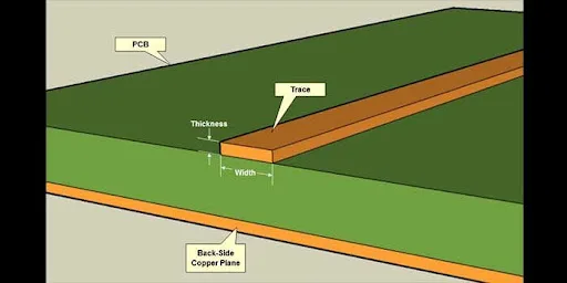
Copper weight in PCBs is measured in ounces per square foot, and 2oz copper means a thicker layer compared to the standard 1oz copper. This added thickness provides several advantages, especially for demanding applications. For instance, 2oz copper can handle higher currents—often up to 4-6 amps per trace, depending on width—without overheating. It also dissipates heat more effectively, reducing the risk of thermal stress in components.
In high-frequency designs, thicker copper helps maintain signal integrity by reducing resistive losses. This is critical for applications like RF circuits where signal degradation can impact performance. Additionally, 2oz copper enhances the mechanical strength of the board, making it more durable in harsh environments such as automotive or industrial settings.
However, while the benefits are clear, the road to successful fabrication with 2oz copper is not always smooth. Let’s explore the key PCB fabrication challenges that arise when working with this material.
Key Challenges in 2oz Copper PCB Manufacturing
Designing with 2oz copper introduces several manufacturing complexities that can affect the quality and cost of the final product. Below, we break down the most common issues and explain why they occur.
1. Fine-Line Etching Difficulties
One of the biggest hurdles in 2oz copper PCB manufacturing is achieving precise fine-line etching. Since the copper layer is thicker, it takes longer to etch away unwanted material during the fabrication process. This extended etching time can lead to undercutting, where the etchant removes copper beneath the resist layer, resulting in wider traces than intended. For designs requiring trace widths as narrow as 4-6 mils (0.004-0.006 inches), this can compromise accuracy and lead to signal integrity issues.
Moreover, thicker copper can create uneven etching rates across the board, especially in densely packed areas. This inconsistency can cause variations in trace width and spacing, impacting the overall performance of high-speed circuits.
2. Increased Material and Processing Costs
Using 2oz copper naturally increases material costs compared to 1oz copper. The raw copper itself is more expensive, and the thicker layer often requires more robust substrates to support it, adding to the expense. Additionally, the longer etching times and specialized equipment needed for processing thicker copper can drive up fabrication costs by 20-30% in some cases.
3. Thermal and Mechanical Stress During Fabrication
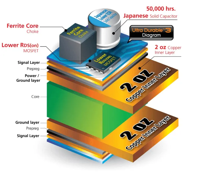
Thicker copper layers are more prone to thermal and mechanical stress during manufacturing processes like lamination and soldering. For example, the coefficient of thermal expansion (CTE) mismatch between the copper and the substrate material (often FR-4) can lead to warping or delamination if not carefully managed. This is particularly problematic in multi-layer boards where internal copper layers are 2oz thick.
4. Impedance Control Challenges
For high-frequency designs, maintaining consistent impedance is critical. With 2oz copper, the thicker traces can alter the dielectric properties between layers, making it harder to achieve the target impedance values (often in the range of 50-100 ohms for RF applications). This requires precise control over trace width, spacing, and dielectric thickness during design and fabrication.
Effective Techniques for Overcoming 2oz Copper Manufacturing Challenges
While the challenges of 2oz copper PCB manufacturing are significant, they are not insurmountable. By adopting the right design strategies and PCB manufacturing techniques, you can achieve high-quality results. Here are some proven methods to address the issues discussed above.
1. Optimizing Fine-Line Etching Processes
To tackle the difficulties of fine-line etching with 2oz copper, consider the following approaches:
- Use Advanced Etching Solutions: Opt for chemical etching solutions specifically formulated for thicker copper. Alkaline etchants, for instance, provide better control and uniformity compared to acidic solutions when dealing with 2oz layers.
- Adjust Etching Parameters: Fine-tune the etching time and temperature to minimize undercutting. Modern fabrication facilities often use automated systems to monitor and adjust these parameters in real-time.
- Implement Tighter Design Rules: Increase the minimum trace width and spacing in your design to account for potential etching variations. For 2oz copper, a minimum trace width of 6 mils and spacing of 8 mils is often recommended for reliable results.
By working closely with your fabrication partner, you can ensure that the etching process is optimized for precision, even with thicker copper layers.
2. Managing Costs Through Smart Design Choices
While 2oz copper inherently costs more, you can mitigate expenses through efficient design practices:
- Selective Copper Weight: Use 2oz copper only in areas of the board that require high current or thermal management, such as power traces. For signal layers, standard 1oz copper may suffice, reducing overall material costs.
- Optimize Board Size: Minimize the board dimensions to reduce the amount of copper and substrate material needed. A smaller footprint can significantly lower costs without compromising functionality.
3. Reducing Thermal and Mechanical Stress
To prevent warping and delamination during fabrication, consider these tips:
- Choose Compatible Materials: Select a substrate with a CTE that closely matches that of copper. High-Tg FR-4 or polyimide materials are often better suited for 2oz copper designs.
- Balance Copper Distribution: Ensure even copper distribution across the board to avoid stress concentration. Use copper pours or dummy fills in empty areas to maintain uniformity.
- Control Lamination Parameters: Work with your manufacturer to optimize lamination temperature and pressure. For 2oz copper, slower heating and cooling cycles can help reduce thermal stress.
4. Achieving Precise Impedance Control
For high-frequency applications, impedance control is non-negotiable. Here’s how to manage it with 2oz copper:
- Use Simulation Tools: Leverage PCB design software to simulate impedance based on trace geometry and dielectric properties. Adjust trace width and spacing to hit target values like 50 ohms for single-ended traces or 100 ohms for differential pairs.
- Tighten Fabrication Tolerances: Specify tighter tolerances for trace width and dielectric thickness during manufacturing. For example, aim for a tolerance of ±10% on trace width to ensure consistency.
- Collaborate with Fabricators: Provide detailed stack-up information to your manufacturer and request impedance testing on prototypes to verify performance before full-scale production.
Best Practices for Designing with 2oz Copper
Beyond addressing specific challenges, following general best practices can streamline the design and manufacturing process for 2oz copper PCBs. These tips will help ensure your project stays on track from concept to production.
- Start with a Robust Design Review: Before sending your design for fabrication, conduct a thorough design rule check (DRC) to identify potential issues like insufficient trace spacing or unbalanced copper distribution.
- Prototype Early: Build and test a prototype to validate your design choices. This step can uncover manufacturing issues like etching inaccuracies or thermal stress before mass production.
- Communicate with Your Manufacturer: Share detailed specifications and discuss your requirements for 2oz copper early in the process. A good fabrication partner will provide feedback on design adjustments to improve manufacturability.
- Document Everything: Maintain clear documentation of your design files, stack-up details, and material specifications. This reduces the risk of miscommunication during fabrication.
Applications of 2oz Copper PCBs
Understanding where 2oz copper excels can help you decide if it’s the right choice for your project. Some common applications include:
- Power Electronics: Used in power supplies and converters where high current capacity (up to 5 amps per trace) is essential.
- Automotive Systems: Ideal for control units and battery management systems that require durability and thermal management.
- Industrial Controls: Suitable for heavy-duty equipment operating in harsh environments with significant heat and vibration.
- RF and High-Frequency Designs: Helps maintain signal integrity in communication devices and radar systems by minimizing resistive losses.
Conclusion: Mastering 2oz Copper PCB Design and Manufacturing
Designing with 2oz copper offers undeniable advantages for high-current and high-frequency applications, but it also demands careful attention to PCB fabrication challenges. From mastering fine-line etching to controlling costs and ensuring impedance accuracy, the journey requires a blend of smart design practices and advanced PCB manufacturing techniques.
By optimizing your etching processes, selecting the right materials, and collaborating closely with your fabrication partner, you can overcome the hurdles of 2oz copper PCB manufacturing and achieve reliable, high-performance results. Whether you’re working on power electronics or RF systems, these strategies will help you navigate the complexities and bring your designs to life.
At ALLPCB, we’re committed to supporting engineers with the tools and expertise needed to succeed in challenging projects like these. With the right approach, 2oz copper can elevate your PCB designs to new heights of performance and durability.


