 ALLPCB


If you're looking to design reliable flex-to-install PCBs for static applications, you're in the right place. These flexible circuit boards, often bent into position once during installation and left static afterward, require specific design considerations to ensure durability and performance. In this guide, we'll cover essential best practices for static flex PCB design, bend-to-install PCB guidelines, and key factors like material selection and stackup design to maximize flexible circuit board reliability.
At ALLPCB, we understand the unique challenges of designing flex PCBs for static applications. Whether you're working on consumer electronics, medical devices, or industrial equipment, this comprehensive blog will walk you through actionable tips to create robust and long-lasting designs. Let's dive into the details of crafting reliable flex-to-install PCBs.
What Are Flex-to-Install PCBs for Static Applications?
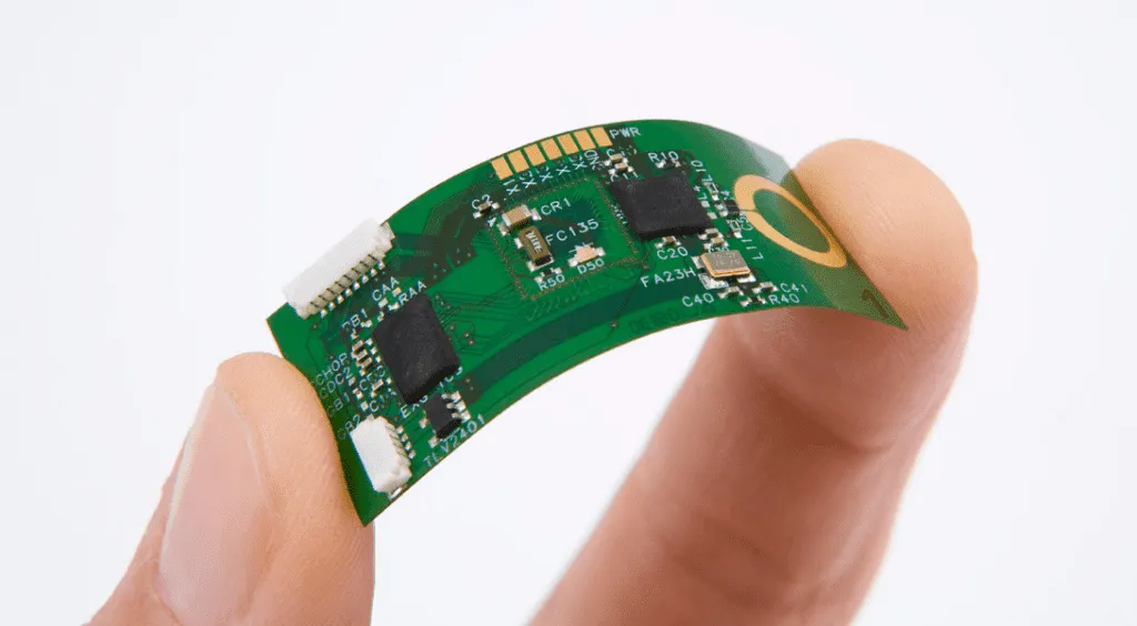
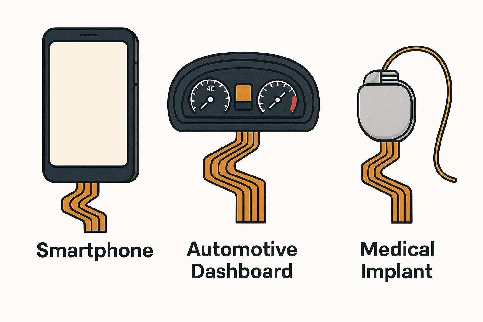
Flex-to-install PCBs, also known as bend-to-install PCBs, are flexible circuit boards designed to be bent or shaped during assembly and remain in a fixed position throughout their operational life. Unlike dynamic flex PCBs, which endure repeated bending, static flex PCBs are meant for one-time installation. Common uses include connecting components in tight spaces, replacing bulky wiring harnesses, or fitting into compact enclosures in devices like cameras, wearables, or automotive systems.
The primary challenge in static flex PCB design is ensuring the board withstands the initial bend without damage while maintaining reliability over time. Factors such as material choice, bend radius, and stackup design play a critical role in achieving this balance. Below, we'll explore best practices to address these challenges and ensure your designs are both functional and durable.
Key Considerations for Static Flex PCB Design
Designing a flex PCB for static applications requires attention to detail to prevent mechanical stress, electrical failures, or long-term degradation. Here are the core principles to follow for optimal performance.
1. Understand Bend Requirements and Constraints
Before diving into the design, analyze the specific bend requirements of your application. For static flex PCBs, the bend is a one-time event, but it must be executed without cracking traces, delaminating layers, or causing other damage. Consider the following:
- Bend Radius: The bend radius should be at least 6-10 times the thickness of the flex PCB for static applications. For example, a 0.2 mm thick board should have a minimum bend radius of 1.2-2 mm to avoid stressing the copper traces.
- Bend Location: Plan the bend area away from critical components or vias to minimize risk. Use design software to simulate the bend and identify potential stress points.
- Strain Relief: Incorporate strain relief features, such as curved traces or wider copper paths, in the bend region to distribute stress evenly.
2. Prioritize Flexible Circuit Board Reliability
Reliability is paramount for flex PCBs in static applications, as they must maintain performance over the product's lifespan without repeated flexing as a variable. To enhance flexible circuit board reliability, focus on these aspects:
- Trace Design: Use wider traces (at least 0.15-0.2 mm for standard designs) in the bend area to reduce the risk of cracking. Avoid placing vias or pads in the bend zone, as they can create weak points.
- Copper Weight: Opt for lighter copper weights, such as 0.5 oz or 1 oz per square foot, to improve flexibility and reduce stress during bending. Heavier copper (e.g., 2 oz) can be more prone to fatigue.
- Adhesive Layers: Choose adhesive-less materials when possible, as adhesives can degrade over time under environmental stress like heat or humidity.
By focusing on these design elements, you can ensure your flex PCB withstands the initial installation and performs reliably in the long term.
Flex PCB Material Selection for Static Applications
Material selection is a critical factor in designing reliable flex-to-install PCBs. The materials must balance flexibility, durability, and electrical performance while meeting the needs of a static application. Here's what to consider when choosing materials:
1. Base Substrate Materials
The most common base material for flex PCBs is polyimide (PI), known for its excellent thermal stability and flexibility. For static applications, standard polyimide films with a thickness of 25-50 micrometers are often ideal, as they provide sufficient flexibility for a one-time bend while maintaining structural integrity.
- Polyimide Benefits: Withstands temperatures up to 260°C, resists chemical degradation, and offers good dielectric properties (dielectric constant around 3.5 at 1 MHz).
- Alternatives: For cost-sensitive projects, polyester (PET) films can be used, though they have lower thermal resistance (up to 150°C) and are less durable.
2. Copper Foil Type
The type of copper foil used in your flex PCB impacts both flexibility and reliability. Rolled annealed (RA) copper is the preferred choice for flex PCBs due to its superior flexibility compared to electrodeposited (ED) copper.
- RA Copper: Offers better ductility and can endure bending without cracking. It’s ideal for static flex designs where the board is shaped once.
- Thickness: Use thinner copper layers (e.g., 9-18 micrometers) to enhance flexibility while ensuring adequate current-carrying capacity (consult design calculators for specific ampacity needs).
3. Coverlay and Protective Layers
Coverlay, a protective layer applied over the copper traces, is essential for insulation and environmental protection in static flex PCBs. Polyimide coverlay is standard, with thicknesses ranging from 25-50 micrometers, providing a balance of protection and flexibility.
- Application Tip: Ensure the coverlay extends beyond the bend area to protect traces from environmental exposure or mechanical damage.
- Stiffeners: Add stiffeners (made of FR4 or polyimide) in non-bend areas to support connectors or components, improving overall reliability.
Flex PCB Stackup Design for Static Applications
The stackup design of a flex PCB defines its layer structure and significantly impacts performance, flexibility, and manufacturability. For static applications, the goal is to keep the design simple and optimized for a single bend. Here's how to approach flex PCB stackup design for static applications:
1. Keep Layer Count Minimal
For static flex PCBs, a single-layer or double-layer design is often sufficient, as these boards typically don’t require complex routing. Fewer layers reduce thickness, improve flexibility, and lower costs.
- Single-Layer Example: A basic stackup might include a polyimide base (25 micrometers), RA copper (18 micrometers), and a polyimide coverlay (25 micrometers), totaling around 0.07-0.08 mm in thickness.
- Double-Layer Consideration: If additional routing is needed, a double-layer stackup can be used, but ensure balanced construction to avoid uneven stress during bending.
2. Balance the Stackup for Stress Distribution
An unbalanced stackup can lead to warping or uneven stress in the bend area. For static flex designs, aim for symmetry in material thickness and placement of copper layers.
- Balanced Design Tip: Place copper layers equidistant from the neutral axis (centerline of the board) to minimize strain during bending. For example, in a double-layer board, ensure copper on both sides is of equal weight.
- Neutral Axis Focus: The neutral axis should ideally pass through the center of the stackup to reduce tension and compression on copper traces during bending.
3. Incorporate Stiffeners in Non-Flex Areas
Stiffeners are often added to static flex PCBs to provide mechanical support in areas that house connectors or components. Use materials like FR4 (0.2-0.5 mm thick) or thicker polyimide to reinforce these regions without compromising the flex area.
Bend-to-Install PCB Guidelines for Success
Following bend-to-install PCB guidelines ensures your flex PCB can be installed without damage and performs reliably in its static state. Here are practical tips to guide your design and assembly process:
1. Design with Assembly in Mind
Work closely with your assembly team to understand how the PCB will be installed. Consider the following:
- Tooling Holes: Add tooling holes or alignment marks outside the bend area to assist with precise installation.
- Bend Angle: Limit the bend angle to 90 degrees or less for static applications to reduce stress on the board. Sharper bends increase the risk of trace damage.
2. Test Prototypes Before Production
Before mass production, create prototypes to test the bend process. Simulate the installation environment to ensure the board can handle the required shape without issues. For instance, if the design requires a 2 mm bend radius, physically bend the prototype to confirm that traces remain intact and no delamination occurs.
3. Document Installation Instructions
Provide clear instructions for the assembly team on how to handle and install the flex PCB. Specify the minimum bend radius, acceptable bend angles, and any areas to avoid stressing. This reduces the likelihood of errors during installation.
Common Challenges and Solutions in Static Flex PCB Design
Even with careful planning, static flex PCB design can present challenges. Here are some common issues and how to address them:
- Challenge: Trace Cracking During Bending
Solution: Increase trace width in the bend area to at least 0.2 mm and use RA copper for better ductility. Avoid sharp corners in trace routing—opt for smooth, curved paths instead. - Challenge: Material Fatigue Over Time
Solution: Select high-quality polyimide materials with proven durability and ensure the coverlay protects all exposed traces from environmental factors. - Challenge: Misalignment During Installation
Solution: Incorporate alignment features like tooling holes or fiducials to guide precise bending and placement during assembly.
Why Choose ALLPCB for Your Static Flex PCB Needs?
At ALLPCB, we specialize in providing high-quality manufacturing and support for flex PCBs tailored to static applications. Our advanced production capabilities ensure precise material selection, accurate stackup designs, and reliable performance for your bend-to-install projects. With a focus on quality and customer satisfaction, we’re here to help bring your designs to life with efficiency and precision.
Conclusion: Mastering Static Flex PCB Design
Designing reliable flex-to-install PCBs for static applications doesn’t have to be daunting. By following best practices for static flex PCB design, adhering to bend-to-install PCB guidelines, and focusing on flexible circuit board reliability, you can create durable and efficient designs. Pay close attention to flex PCB material selection for static applications and optimize your flex PCB stackup design to balance flexibility and strength.
With these strategies in mind, you’re well-equipped to tackle the challenges of static flex PCB design and deliver products that stand the test of time. Trust ALLPCB to support your journey with top-tier manufacturing solutions and expertise in flexible circuit technology.


