 ALLPCB


If you're looking for the best way to separate individual printed circuit boards (PCBs) from a larger panel, the right depaneling method depends on your panel size, board design, and production needs. Whether you're dealing with small, intricate panels or large, high-volume batches, options like V-cut, tab routing, laser depaneling, and manual separation each have unique benefits and challenges. In this comprehensive guide, we'll break down these PCB depaneling methods, compare their suitability for different panel sizes, and help you make an informed choice for your project.
What Is PCB Depaneling and Why Does It Matter?
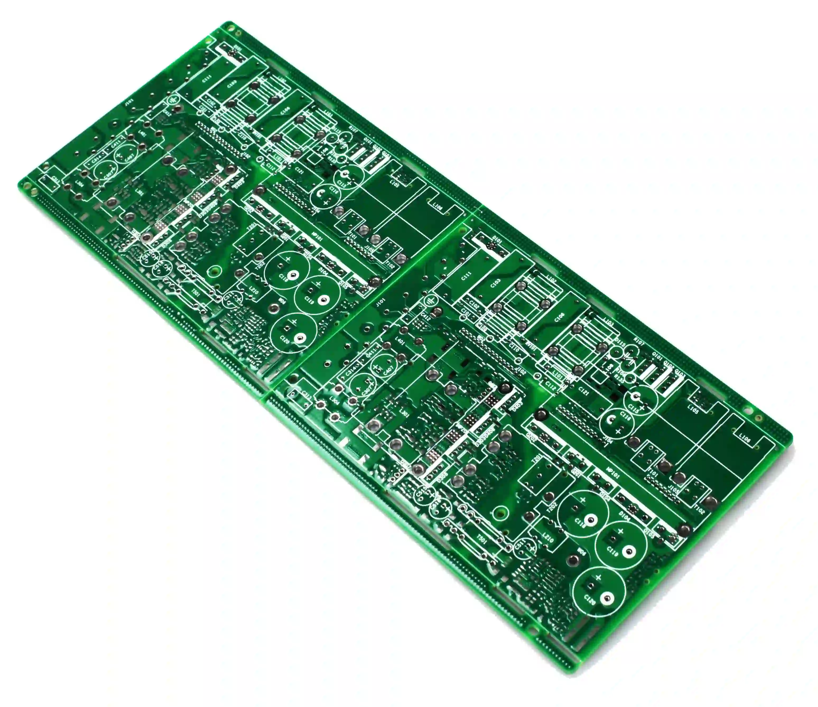
PCB depaneling, also known as PCB panel separation, is the process of separating individual circuit boards from a larger panel after manufacturing. Panels are used to streamline production, allowing multiple boards to be fabricated and assembled at once, which saves time and reduces costs. However, separating these boards without damaging components or compromising quality is critical.
Choosing the right depaneling method impacts production efficiency, board integrity, and overall cost. A poor choice can lead to micro-cracks in solder joints, damaged components, or wasted materials. Factors like panel size, board thickness, and component placement near edges play a significant role in determining the best approach. Let’s explore the most common PCB depaneling methods and how they suit different panel sizes and project requirements.
Understanding PCB Panel Sizes and Their Challenges
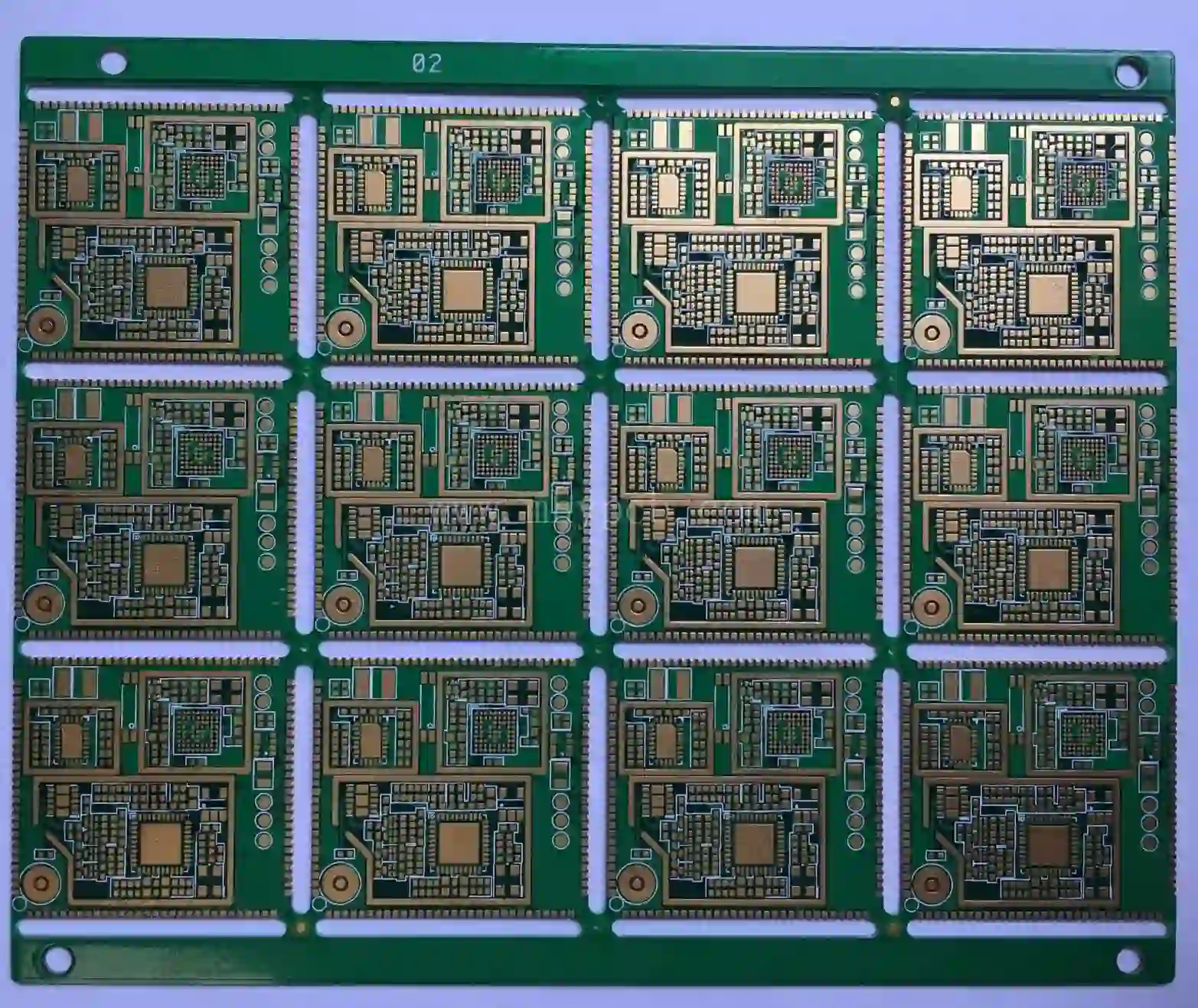
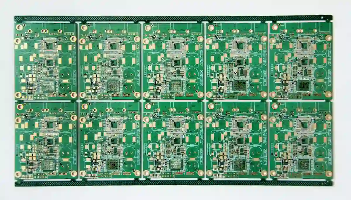
PCB panels come in a wide range of sizes, from small panels of just a few inches for compact devices to large panels over 20 inches for industrial applications. The size of the panel often dictates the depaneling method due to factors like handling ease, stress on the board, and precision requirements.
- Small Panels (under 6 inches): These are often used for compact electronics like wearables or IoT devices. They require high precision to avoid damaging tiny components near edges.
- Medium Panels (6-12 inches): Common for consumer electronics, these panels balance precision and volume, often needing methods that support moderate production speeds.
- Large Panels (over 12 inches): Used in industrial or automotive applications, these panels prioritize efficiency and durability during separation due to their size and thickness.
Each size category presents unique challenges, such as managing mechanical stress on larger panels or ensuring clean cuts on smaller, densely populated boards. Let’s dive into the primary PCB depaneling methods to see how they align with these needs.
Common PCB Depaneling Methods Explained
1. V-Cut Depaneling: Simple and Cost-Effective
V-cut depaneling involves creating V-shaped grooves along the separation lines of a PCB panel during manufacturing. These grooves, typically one-third the thickness of the board (e.g., 0.4 mm for a 1.2 mm thick board), weaken the material, allowing the boards to be snapped apart by hand or with a simple tool.
Best for: Small to medium panels with straight separation lines and low to moderate production volumes. It’s ideal for panels up to 12 inches where components are not placed closer than 0.5 mm to the V-cut line to avoid stress-related damage.
Advantages:
- Low cost, as it requires minimal equipment.
- Fast for small batches, often taking just seconds per panel.
- Suitable for simple rectangular board shapes.
Limitations:
- Not suitable for complex board shapes or curved edges.
- Can cause mechanical stress, risking micro-cracks in solder joints if components are too close to the cut line.
- Less effective for large panels over 12 inches due to uneven stress distribution during snapping.
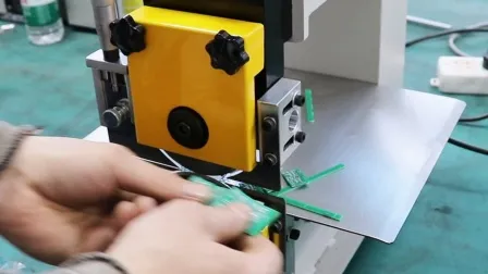
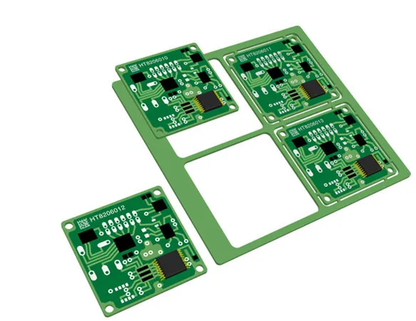
2. Tab Routing: Flexible for Complex Shapes
Tab routing, also known as breakaway tab depaneling, uses small, perforated tabs to hold individual PCBs together within a panel. These tabs are strategically placed along the edges and can be broken off manually or with a tool after assembly. The tabs are often 2-3 mm wide, with perforations reducing their strength for easier separation.
Best for: Medium to large panels with irregular or non-rectangular board shapes. It works well for panels up to 18 inches and is often used when V-cuts can’t accommodate the design.
Advantages:
- Supports complex board shapes and curved edges.
- Reduces mechanical stress compared to V-cut, as tabs can be placed away from critical components.
- Effective for larger panels where uniform snapping is challenging.
Limitations:
- Leaves small tab remnants on board edges, which may require additional cleanup for aesthetic or functional reasons.
- Tab placement must be carefully designed to ensure panel stability during assembly.
- Slower than V-cut for high-volume production due to manual removal of tabs.
Suggested Reading: Mastering Tab Routing: Techniques for Clean and Stress-Free PCB Depaneling
3. Laser Depaneling: Precision for High-Tech Needs
Laser depaneling uses a focused laser beam, often a UV laser with a wavelength of 355 nm, to cut through PCB material with extreme precision. This method is contactless, meaning it applies no mechanical stress to the board. Cutting speeds can range from 100-500 mm per second, depending on material thickness and laser power.
Best for: Small to medium panels with dense component layouts or high precision requirements. It’s ideal for panels under 10 inches where components are as close as 0.1 mm to the cut line.
Advantages:
- Offers unmatched precision, with tolerances as tight as 0.02 mm.
- No mechanical stress, preventing damage to delicate components or solder joints.
- Handles complex shapes and thin materials (down to 0.1 mm thickness) with ease.
Limitations:
- High initial equipment cost and slower processing times for thicker materials (over 1.6 mm).
- Not cost-effective for large panels or high-volume production due to longer cutting times.
- Requires specialized safety measures and ventilation for fumes produced during cutting.
4. Manual Depaneling: Basic but Limited
Manual depaneling involves using hand tools like shears, cutters, or even just breaking boards by hand along pre-scored lines. It’s the simplest method and requires no sophisticated equipment, often relying on basic scoring done during manufacturing.
Best for: Very small panels or prototypes with low production volumes. It’s practical for panels under 6 inches where precision and speed are not critical.
Advantages:
- Extremely low cost, requiring only basic tools.
- Quick setup for one-off projects or small batches.
- No need for specialized equipment or training.
Limitations:
- High risk of damage to boards and components due to inconsistent force application.
- Not suitable for medium or large panels due to difficulty in maintaining clean separation.
- Time-consuming and labor-intensive for anything beyond a few panels.
V-Cut vs. Tab Routing: Which Is Better for Your Panel Size?
When deciding between V-cut and tab routing, panel size and design complexity are key considerations. Let’s compare them directly:
- Panel Size Suitability: V-cut works best for small to medium panels (under 12 inches) with straight edges, while tab routing is more versatile for medium to large panels (up to 18 inches) and complex shapes.
- Stress and Component Safety: V-cut can introduce stress near the cut line, risking damage if components are closer than 0.5 mm. Tab routing minimizes stress by allowing tabs to be placed away from critical areas.
- Production Speed: V-cut is faster for simple designs and smaller batches, as snapping can be done in seconds. Tab routing takes longer due to tab removal but offers better control for larger panels.
For example, if you’re working on a 10-inch panel for a consumer device with rectangular boards, V-cut might be the most cost-effective choice. However, for a 15-inch panel with irregular board shapes for an automotive application, tab routing would provide the flexibility and safety needed.
Suggested Reading: V-Scoring vs. Stamp Hole Depaneling: Choosing the Right Method for Your PCB
How Panel Size Influences Depaneling Method Choice
Panel size directly affects the practicality and efficiency of each depaneling method. Here’s a breakdown of how to choose based on size:
- Small Panels (under 6 inches): Laser depaneling or manual depaneling are often best. Laser offers precision for dense layouts common in small boards, while manual separation suits prototypes or low-budget projects.
- Medium Panels (6-12 inches): V-cut and tab routing shine here. V-cut is ideal for straightforward designs, while tab routing handles more complex layouts without sacrificing board integrity.
- Large Panels (over 12 inches): Tab routing is typically the go-to method due to its ability to manage stress across larger areas. Laser depaneling is rarely used for large panels due to cost and time constraints.
Additionally, consider board thickness alongside size. Thicker boards (over 1.6 mm) may struggle with laser cutting efficiency, while thinner boards (under 0.8 mm) are more prone to damage during V-cut or manual separation.
Key Factors Beyond Size to Consider
While panel size is a major factor, other elements also influence the best depaneling method:
- Component Proximity: If components are within 0.5 mm of the edge, laser depaneling is safest to avoid stress-related damage.
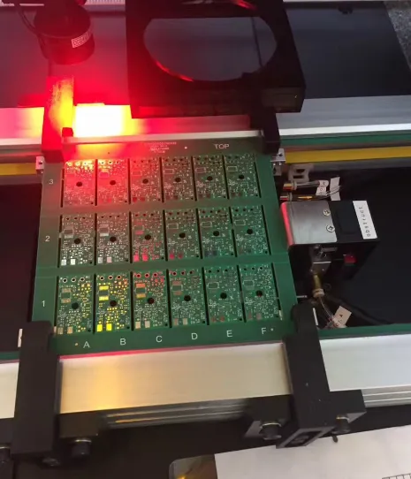
- Production Volume: High-volume runs benefit from automated methods like V-cut or tab routing with machine assistance, while low volumes can rely on manual or laser methods for flexibility.
- Board Material: FR4, the most common PCB material, works with all methods, but flexible or ceramic boards may require laser cutting for clean results.
- Budget: Manual and V-cut methods are the most affordable, while laser depaneling involves higher upfront costs but delivers precision for critical applications.
Tips for Optimizing Your Depaneling Process
To ensure a smooth depaneling process regardless of the method chosen, follow these practical tips:
- Design panels with depaneling in mind by leaving adequate spacing (at least 0.5 mm) between components and cut lines.
- For V-cut, ensure groove depth is consistent (typically one-third of board thickness) to avoid uneven snapping.
- When using tab routing, place tabs in non-critical areas and test panel stability during assembly to prevent premature breakage.
- For laser depaneling, collaborate with your manufacturer to optimize cutting paths, reducing processing time and cost.
- Always inspect separated boards for edge quality and test for micro-cracks, especially with mechanical methods like V-cut or manual separation.
Conclusion: Making the Right Choice for PCB Depaneling
Selecting the right PCB depaneling method for your panel size is crucial to maintaining board quality, minimizing production costs, and meeting project deadlines. Small panels often benefit from the precision of laser depaneling or the simplicity of manual separation, while medium panels suit V-cut or tab routing for efficiency. Large panels typically require tab routing to handle stress and complex designs effectively.
By understanding the strengths and limitations of each method—V-cut, tab routing, laser depaneling, and manual separation—you can align your choice with your specific needs. Factor in panel size, board design, component layout, and production volume to ensure a seamless depaneling process. With the right approach, you’ll achieve clean separations, protect your boards, and optimize your manufacturing workflow.
At ALLPCB, we’re committed to supporting your PCB projects with tailored solutions and expert guidance. Whether you’re navigating PCB panel separation challenges or refining your design for depaneling, our team is here to help you succeed.


