ALLPCB


If you're a PCB designer, you've likely heard various claims about copper cladding—some praising its benefits, others warning of its downsides. But how much of this information is fact, and how much is myth? In this comprehensive guide, we’ll debunk common myths surrounding copper cladding, focusing on key areas like copper cladding oxidation, corrosion resistance, thermal conductivity, and cost analysis. Whether you're designing for high-frequency applications or cost-sensitive projects, understanding the truth about copper cladding can save you time, money, and design headaches.
Let’s dive into the facts and clear up the misconceptions so you can make informed decisions for your next PCB project with confidence.
What Is Copper Cladding in PCB Design?
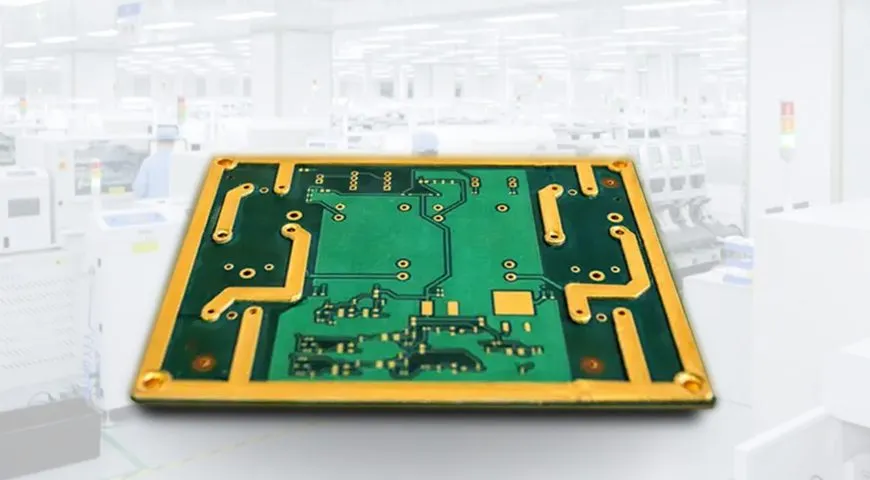
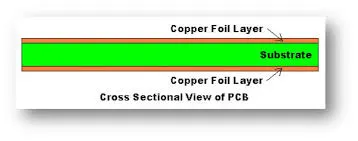
Copper cladding refers to the layer of copper foil bonded to the substrate of a printed circuit board (PCB). This layer forms the conductive traces and pads that carry electrical signals across the board. Typically, copper cladding is applied to one or both sides of the PCB substrate, such as FR4, and comes in various thicknesses, often measured in ounces per square foot (oz/ft2). For instance, 1 oz/ft2 copper is about 35 micrometers thick and is a common choice for standard designs.
Copper is chosen for its excellent electrical conductivity, which ensures minimal signal loss, and its ability to handle current efficiently. However, myths and misunderstandings about copper cladding often lead designers to overestimate its limitations or undervalue its benefits. Let’s tackle these myths head-on, focusing on oxidation, corrosion resistance, thermal conductivity, and cost.
Myth 1: Copper Cladding Oxidation Ruins PCB Performance
One of the most persistent myths is that copper cladding oxidation will inevitably degrade a PCB’s performance over time. While it’s true that copper can oxidize when exposed to air, forming a layer of copper oxide, the reality is far less alarming than many believe.
Copper oxide forms as a thin, greenish layer (often called patina) on the surface of copper when it reacts with oxygen and moisture. However, in most PCB applications, this oxidation is minimal and does not significantly impact electrical performance. The reason? Most copper cladding on PCBs is protected by solder masks or surface finishes like HASL (Hot Air Solder Leveling), ENIG (Electroless Nickel Immersion Gold), or OSP (Organic Solderability Preservative). These finishes act as barriers, preventing direct exposure to environmental factors that cause oxidation.
In high-reliability applications, such as aerospace or medical devices, where even minor oxidation could pose a risk, designers often opt for gold or nickel plating over copper. For standard consumer electronics, however, oxidation is rarely a concern when proper manufacturing and storage practices are followed. Studies show that a properly finished PCB can maintain its integrity for years, with signal loss due to oxidation being negligible—often less than 0.1% over a decade under normal conditions.
Key Takeaway: Copper cladding oxidation is not a significant threat to PCB performance when protective finishes are applied. Focus on selecting the right surface finish for your application to ensure long-term reliability.
Myth 2: Copper Cladding Has Poor Corrosion Resistance
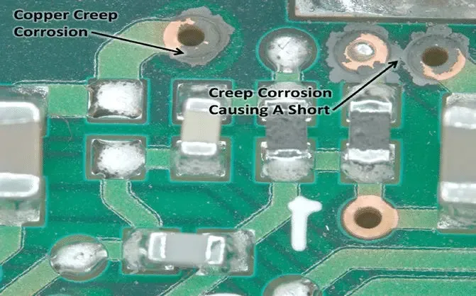
Another common misconception is that copper cladding offers poor corrosion resistance, making it unsuitable for harsh environments. While copper is not as corrosion-resistant as metals like stainless steel, it performs admirably in most PCB applications when handled correctly.
Copper cladding corrosion resistance depends on the environment and the protective measures in place. In humid or salty conditions, such as coastal areas, unprotected copper can corrode faster due to the presence of chloride ions. However, as with oxidation, modern PCB manufacturing techniques mitigate this risk. Solder masks, conformal coatings, and surface finishes shield the copper from moisture and contaminants, significantly extending its lifespan.
For extreme environments, such as automotive or industrial applications, designers can specify thicker copper layers or additional protective coatings. For example, a 2 oz/ft2 copper layer (approximately 70 micrometers thick) provides greater durability than a 1 oz/ft2 layer, reducing the risk of corrosion-related failures. Additionally, conformal coatings like acrylic or silicone can provide an extra barrier, ensuring corrosion resistance even in temperatures ranging from -40°C to 85°C and humidity levels up to 95%.
Key Takeaway: Copper cladding corrosion resistance is adequate for most applications when paired with proper protective measures. For harsh environments, consider thicker copper or specialized coatings to enhance durability.
Myth 3: Copper Cladding Thermal Conductivity Is Overrated
Some designers believe that the thermal conductivity of copper cladding is overrated and that it doesn’t significantly impact heat dissipation in PCBs. This myth can lead to poor design choices, especially in high-power applications where thermal management is critical.
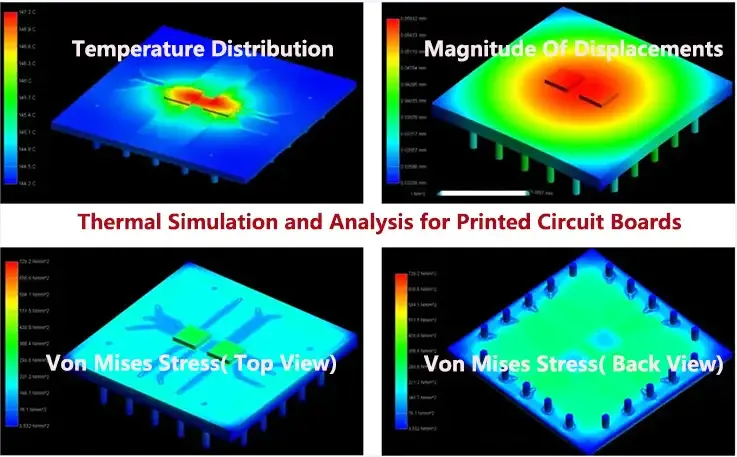
Copper has a thermal conductivity of approximately 401 W/m·K, making it one of the best heat-conducting metals used in electronics. In comparison, aluminum, another common material, has a thermal conductivity of about 237 W/m·K, while FR-4, a typical PCB substrate, is around 0.3 W/m·K. This means copper cladding plays a vital role in dissipating heat away from components, preventing overheating and ensuring reliable operation.
In high-power designs, such as power supplies or LED drivers, thicker copper cladding (e.g., 3 oz/ft2 or higher) is often used to handle higher current densities and improve heat dissipation. For instance, a PCB with 3 oz/ft2 copper can manage current densities up to 30 A/mm2 without significant temperature rise, compared to 10 A/mm2 for 1 oz/ft2 copper. This capability is essential for preventing thermal runaway in densely packed circuits.
However, thermal conductivity isn’t a one-size-fits-all solution. Designers must also consider the overall thermal design, including vias, heat sinks, and component placement, to maximize heat dissipation. Copper cladding alone won’t solve all thermal issues, but it is a critical factor that should not be underestimated.
Key Takeaway: Copper cladding thermal conductivity is a significant advantage in managing heat in PCB designs. Use thicker copper layers and complementary thermal management strategies for high-power applications.
Myth 4: Copper Cladding Cost Is Always Prohibitive
Finally, many designers assume that using copper cladding, especially thicker layers, is always expensive and not worth the investment. A proper copper cladding cost analysis reveals that this isn’t necessarily true—it depends on the application and design requirements.
The cost of copper cladding is influenced by several factors, including the thickness of the copper layer, the size of the PCB, and the volume of production. For example, a 1 oz/ft2 copper layer is standard and relatively inexpensive, often adding just a few cents per square inch to the overall cost of a small-batch PCB. Moving to 2 oz/ft2 or 3 oz/ft2 copper increases the cost by approximately 20-50% per layer, depending on the manufacturer and order quantity. For high-volume production, this cost per unit drops significantly due to economies of scale.
Thicker copper is often necessary for high-current applications, where the cost is justified by improved performance and reliability. For instance, in an automotive power module, using 3 oz/ft2 copper might add $1-2 to the cost of each board but can prevent failures that would cost thousands in recalls or repairs. On the other hand, for low-power consumer devices, sticking with 1 oz/ft2 copper keeps costs down without sacrificing functionality.
Another cost-saving tip is to optimize the design to minimize copper usage where high thickness isn’t needed. For example, use thicker copper only on power traces and standard thickness on signal traces. This hybrid approach balances performance and cost effectively.
Key Takeaway: Copper cladding cost analysis shows that thicker copper isn’t always expensive when weighed against the benefits in specific applications. Optimize your design to use thicker copper only where necessary to manage costs.
Practical Tips for Working with Copper Cladding in PCB Design
Now that we’ve debunked the major myths, here are some practical tips to help you make the most of copper cladding in your PCB designs:
- Choose the Right Thickness: Select copper thickness based on current requirements. Use 1 oz/ft2 for standard designs, and scale up to 2 or 3 oz/ft2 for high-current or high-power applications.
- Prioritize Surface Finishes: Protect against copper cladding oxidation and corrosion by choosing appropriate finishes like ENIG or OSP, especially for long-term reliability.
- Focus on Thermal Management: Leverage copper cladding thermal conductivity by pairing it with thermal vias and heat sinks in high-power designs to prevent overheating.
- Balance Cost and Performance: Conduct a copper cladding cost analysis to determine where thicker copper is necessary and where standard layers will suffice.
- Test in Real Conditions: Simulate or prototype your design under real-world conditions to ensure that issues like corrosion or thermal buildup won’t affect performance.
By following these guidelines, you can avoid common pitfalls and ensure your PCB designs are both efficient and reliable.
Conclusion: Making Informed Decisions About Copper Cladding
Copper cladding is a cornerstone of PCB design, offering excellent conductivity and versatility. However, myths about copper cladding oxidation, corrosion resistance, thermal conductivity, and cost can lead to misunderstandings and suboptimal design choices. By separating fact from fiction, you can confidently use copper cladding to meet the specific needs of your project—whether it’s a low-cost consumer device or a high-reliability industrial system.
Understanding the true properties of copper cladding allows you to design PCBs that perform better, last longer, and stay within budget. Keep these insights in mind for your next project, and you’ll be well-equipped to tackle any design challenge with clarity and precision.