 ALLPCB


When designing high-voltage printed circuit boards (PCBs), two critical factors ensure safety and reliability: creepage distance and clearance distance. But what exactly are these terms, and why do they matter so much in high-voltage PCB design? Simply put, creepage distance is the shortest path between two conductive parts along the surface of an insulating material, while clearance distance is the shortest path through the air between those parts. Together, they prevent electrical breakdowns, arcing, and safety hazards in high-voltage applications.
In this comprehensive guide, we’ll dive deep into the world of creepage distance high voltage PCB and clearance distance high voltage PCB design. We’ll explore their importance, the standards like IPC-2221 creepage clearance that guide their implementation, and actionable high voltage PCB design rules to help engineers create safe and efficient boards. Whether you’re a seasoned designer or new to high-voltage systems, this blog will equip you with the knowledge to tackle spacing challenges with confidence.
What Are Creepage and Clearance in High-Voltage PCB Design?
Let’s start with the basics. In high-voltage PCB design, creepage and clearance are all about maintaining safe distances between conductive elements to prevent electrical failures. These distances are not just arbitrary numbers—they are carefully calculated based on the voltage levels, environmental conditions, and material properties of the PCB.
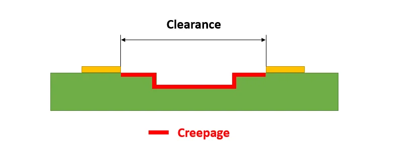
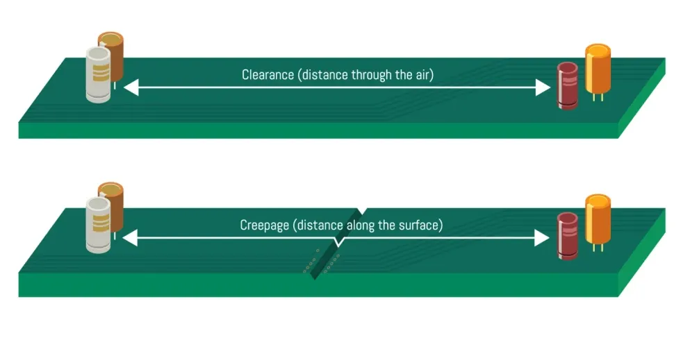
Creepage Distance refers to the shortest distance along the surface of an insulating material (like the PCB substrate) between two conductive parts. This path matters because contaminants like dust, moisture, or pollution can create a conductive layer on the surface, leading to unintended current flow or arcing. For example, in a 500V system, a creepage distance of at least 6.4 mm might be required, depending on the material and environment.
Clearance Distance, on the other hand, is the shortest distance through the air between two conductive parts. This measurement is crucial to prevent electrical arcing, where a high voltage causes a spark to jump through the air. For instance, at 1000V, a clearance of around 8 mm might be necessary in standard atmospheric conditions to avoid breakdown.
Both creepage and clearance are vital to ensure that high-voltage PCBs operate safely without risking short circuits, fires, or damage to components. Ignoring these distances can lead to catastrophic failures, especially in applications like power supplies, industrial equipment, or electric vehicles where voltages can exceed 1000V.
Why Creepage and Clearance Are Critical for High-Voltage PCBs
In high-voltage systems, the stakes are incredibly high. A small oversight in spacing can result in electrical arcing, insulation breakdown, or even personal injury. Here’s why creepage and clearance are the MVPs (Most Valuable Players) of PCB design in these scenarios:
- Safety First: Proper spacing prevents dangerous situations like electric shocks or fires caused by unintended current flow.
- Reliability: Adequate creepage and clearance distances reduce the risk of component failure due to electrical stress, extending the lifespan of the PCB.
- Compliance: Meeting industry standards like IPC-2221 ensures that your design passes regulatory checks and performs reliably in real-world conditions.
- Environmental Factors: Dust, humidity, and altitude can reduce insulation effectiveness. Creepage and clearance distances account for these variables to maintain performance.
For example, in a high-voltage power supply operating at 2000V, failing to maintain a clearance of at least 16 mm (as per typical standards) could result in arcing, damaging nearby components and potentially causing a system-wide failure. Similarly, insufficient creepage distance in a humid environment could allow moisture to create a conductive path, leading to a short circuit.
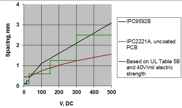
Understanding IPC-2221 Creepage and Clearance Standards
When it comes to defining safe spacing for high-voltage PCBs, the IPC-2221 creepage clearance standard is the go-to reference for many engineers. IPC-2221, titled "Generic Standard on Printed Board Design," provides detailed guidelines for various aspects of PCB design, including electrical spacing requirements.
According to IPC-2221, creepage and clearance distances depend on several factors:
- Voltage Levels: Higher voltages require larger distances. For instance, at 500V, IPC-2221 might recommend a clearance of 6.4 mm for uncoated boards in clean conditions.
- Altitude: Air pressure decreases at higher altitudes, reducing its insulating properties. Designs for equipment used at 3000 meters above sea level may need increased clearance distances compared to sea-level applications.
- Material Group: The insulating material’s ability to resist tracking (surface degradation due to electrical stress) affects creepage distances. Materials are categorized into groups (I, II, IIIa, IIIb) based on their Comparative Tracking Index (CTI), with Group I offering the best resistance.
- Pollution Degree: This measures the level of contamination expected in the operating environment. A pollution degree of 3 (heavy industrial dust or moisture) requires greater creepage distances than a pollution degree of 1 (clean, controlled environments).
IPC-2221 provides tables to help designers determine the minimum creepage and clearance distances. For a 1000V application in a pollution degree 2 environment using a material in Group II, the standard might specify a creepage distance of around 10 mm and a clearance of 8 mm. These values are starting points, and adjustments may be needed based on specific design requirements or additional standards like IEC 60950 for safety in information technology equipment.
High Voltage PCB Design Rules for Creepage and Clearance
Designing a high-voltage PCB requires careful planning to meet creepage and clearance requirements. Below are some practical high voltage PCB design rules to guide you through the process:
1. Know Your Voltage and Environment
Start by identifying the maximum operating voltage of your system, including any transient spikes. A design for a 1500V system, for instance, might need to account for surges up to 2000V. Next, consider the operating environment. Will the PCB be exposed to dust, moisture, or high altitudes? These factors will influence the required spacing.
2. Select the Right Materials
The choice of PCB substrate plays a big role in creepage performance. Materials like FR-4 with a high CTI value (e.g., 400 or above) are better suited for high-voltage applications as they resist surface tracking. Additionally, consider applying conformal coatings to enhance insulation and protect against environmental contaminants.
3. Use Slots and Barriers for Enhanced Isolation
In cases where maintaining large creepage distances is challenging due to board size constraints, adding slots or barriers can help. Cutting a slot in the PCB between high-voltage traces increases the surface distance, effectively boosting creepage. For example, a 2 mm wide slot can add several millimeters to the creepage path without increasing the board’s footprint.
4. Optimize Component Placement
Place high-voltage components strategically to minimize the risk of arcing. Avoid placing sensitive low-voltage components near high-voltage traces. If a 1000V trace runs near a 5V signal line, ensure at least 8 mm of clearance (or more, based on standards) to prevent interference or breakdown.
5. Leverage Design Software Tools
Modern PCB design software often includes features to set and check creepage and clearance rules automatically. Use these tools to define minimum spacing constraints based on IPC-2221 or other standards, ensuring your layout complies before manufacturing.
6. Test for Compliance
After completing your design, perform dielectric strength tests and hipot (high potential) testing to verify that the PCB can withstand the expected voltage without breakdown. For a 2000V system, testing at 1.5 times the operating voltage (3000V) for a specified duration can confirm the adequacy of your spacing.
Common Challenges in Maintaining Creepage and Clearance
While the importance of creepage and clearance is clear, implementing them in real-world designs can be tricky. Here are some common challenges engineers face and how to address them:
- Limited Board Space: High-density designs often leave little room for large spacing. Solutions include using slots, barriers, or multilayer boards to separate high-voltage areas vertically.
- Environmental Variability: A PCB designed for a clean lab environment might fail in a dusty factory. Design with worst-case conditions in mind, and consider protective enclosures or coatings.
- Cost Constraints: High-CTI materials or additional manufacturing steps like slotting can increase costs. Balance safety requirements with budget by optimizing only critical areas of the design.
For instance, in a compact 800V power converter design, achieving a 10 mm creepage distance might seem impossible. By introducing a 1 mm slot between traces and using a high-quality insulating material, the effective creepage path can be extended without significantly enlarging the board.
Practical Examples of Creepage and Clearance in Action
Let’s look at a couple of real-world scenarios to see how creepage and clearance distances are applied in high-voltage PCB design.
Example 1: Industrial Motor Controller
An industrial motor controller operates at 1200V in a factory environment with moderate dust (pollution degree 2). Based on IPC-2221, the design requires a clearance of approximately 9.5 mm and a creepage distance of 12.5 mm for a Group II material. To meet this on a compact board, the designer uses a slot between high-voltage traces and applies a conformal coating to enhance surface insulation.
Example 2: Electric Vehicle Power Module
An electric vehicle power module handles 800V with potential surges to 1000V. Operating in varying humidity levels, the design must account for pollution degree 3. The required creepage distance is around 16 mm, achieved by spacing components farther apart and using a high-CTI substrate. Clearance is set at 8 mm, verified through hipot testing at 1500V to ensure no arcing occurs.
Tips for Balancing Creepage, Clearance, and Design Constraints
Achieving the right creepage and clearance distances often involves trade-offs. Here are some tips to balance safety with practical design needs:
- Prioritize critical areas of the PCB where high voltages are present, and relax spacing in low-voltage sections to save space.
- Use multilayer boards to separate high-voltage traces onto different layers, reducing surface creepage concerns.
- Collaborate with your manufacturing partner to ensure that slots, coatings, or material choices are feasible within production capabilities.
Conclusion: Mastering Creepage and Clearance for Safe High-Voltage Designs
Creepage and clearance are the unsung heroes of high-voltage PCB design. By understanding and applying the principles of creepage distance high voltage PCB and clearance distance high voltage PCB, you can create boards that are safe, reliable, and compliant with standards like IPC-2221 creepage clearance. Following high voltage PCB design rules ensures that your designs withstand the rigors of high-voltage operation, whether in industrial, automotive, or power electronics applications.
From selecting the right materials to using design tools and testing for compliance, every step counts in mastering these critical spacing requirements. With the guidelines and examples provided in this blog, you’re well-equipped to tackle the challenges of high-voltage PCB design and deliver products that perform flawlessly under pressure.


