ALLPCB


When it comes to designing printed circuit boards (PCBs) for space probes, selecting the right materials is crucial. Space environments are harsh, with extreme temperatures, radiation, and vacuum conditions that can degrade standard materials. The key to success lies in choosing space-grade PCB laminate materials, understanding PCB substrate selection for space probes, managing outgassing PCB materials in space, and ensuring compatibility with high-frequency PCB materials for space applications. In this guide, we’ll walk you through the essential factors to consider and provide actionable insights to help you make informed decisions for your space probe projects.
This blog will dive deep into the unique challenges of space environments, the properties of suitable materials, and practical tips for material selection. Whether you’re an engineer working on satellite systems or a designer crafting electronics for deep-space missions, this guide will equip you with the knowledge to build reliable and high-performing PCBs.
Why Material Selection Matters for Space Probe PCBs
Space probes operate in conditions far beyond what typical electronics are designed to handle. Temperatures can swing from -150°C to over 120°C, radiation levels can disrupt electronic signals, and the vacuum of space can cause materials to release gases, potentially damaging sensitive components. Choosing the right materials ensures that PCBs can withstand these challenges, maintain signal integrity, and function reliably over long missions, often spanning years or decades.
For instance, a poorly chosen laminate might crack under thermal stress or release harmful gases (outgassing) that could contaminate optical instruments on a probe. On the other hand, selecting materials specifically engineered for space can prevent these issues, ensuring mission success. Let’s explore the specific challenges and how material selection addresses them.

Key Challenges in Space Environments for PCBs
Before selecting materials, it’s important to understand the unique conditions space probes face. These challenges directly influence the choice of space-grade PCB laminate materials and substrates.
1. Extreme Temperature Variations
Space probes experience drastic temperature changes depending on their exposure to sunlight or shadow. Materials must have low thermal expansion coefficients (CTE) to avoid cracking or delamination. For example, a CTE mismatch between the laminate and copper layers can cause mechanical failure at temperature extremes. Typical space-grade materials are designed to handle ranges from -55°C to +125°C or wider.
2. Radiation Exposure
High-energy radiation in space can degrade materials and interfere with electronic performance. Radiation can cause dielectric breakdown or increase signal noise in PCBs. Materials with high radiation resistance, such as certain polyimides, are often chosen for their ability to maintain structural and electrical integrity under prolonged exposure.
3. Vacuum Conditions and Outgassing
In the vacuum of space, some materials release gases in a process called outgassing. This can lead to contamination of nearby components, such as sensors or lenses, which is a critical concern for space probes. Selecting low-outgassing materials that meet standards like NASA’s ASTM E595 (with Total Mass Loss, TML, less than 1% and Collected Volatile Condensable Material, CVCM, less than 0.1%) is essential.
4. High-Frequency Signal Requirements
Many space probes rely on high-frequency signals for communication and data transmission. Materials must support low dielectric loss (Df) and stable dielectric constant (Dk) to ensure minimal signal attenuation. For example, a Dk value around 3.0 to 3.5 is often ideal for maintaining signal speed and integrity in high-frequency applications.
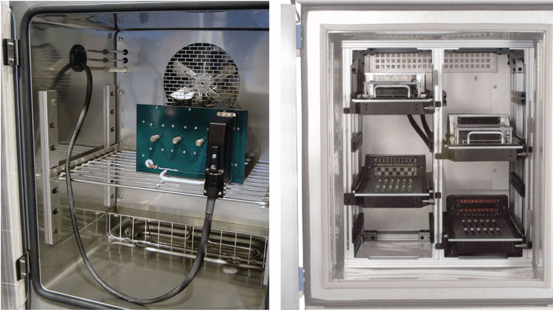
Suggested Image Placement: Insert an image here showing a PCB under thermal stress testing.
ALT Text: "PCB undergoing thermal stress testing for space applications."
Critical Factors in PCB Substrate Selection for Space Probes
Choosing the right substrate is the foundation of designing reliable PCBs for space probes. Here are the key factors to consider during PCB substrate selection for space probes.
1. Thermal Stability
Substrates must endure rapid temperature changes without deforming or losing electrical properties. Polyimide-based laminates are a popular choice due to their high glass transition temperature (Tg), often exceeding 250°C, which ensures stability under thermal stress. For comparison, standard FR-4 materials have a Tg of around 130-140°C, making them unsuitable for space applications.
2. Dielectric Properties
For high-frequency applications, the dielectric constant (Dk) and loss tangent (Df) of the substrate are critical. A low Dk (e.g., 2.2 to 3.5) helps maintain signal speed, while a low Df (e.g., 0.002 to 0.005) reduces signal loss. Materials like PTFE-based laminates are often used in high-frequency PCB materials for space due to their excellent electrical performance.
3. Mechanical Strength
Space probes experience intense vibrations during launch and mechanical stress in orbit. Substrates must have high tensile strength and flexibility to avoid cracking. Polyimide materials, for instance, offer a tensile strength of around 231 MPa, making them robust enough for such conditions.
4. Radiation Hardness
Materials must resist degradation from cosmic rays and solar radiation. Certain ceramics and specialized polyimides are engineered to withstand total ionizing doses (TID) of over 100 krad without significant performance loss, making them ideal for long-term missions.

Addressing Outgassing: Choosing Low-Outgassing PCB Materials for Space
Outgassing is a major concern in space applications, as released gases can condense on sensitive equipment, impairing functionality. When selecting outgassing PCB materials for space, prioritize materials that have been tested and certified for low outgassing under vacuum conditions.
Standards for Low Outgassing
The most widely recognized standard for outgassing is NASA’s ASTM E595 test, which measures Total Mass Loss (TML) and Collected Volatile Condensable Material (CVCM). Materials with TML less than 1% and CVCM less than 0.1% are considered safe for space use. Many space-grade epoxies and polyimides meet these criteria.
Material Options
Polyimide films and certain silicone-free adhesives are known for their low outgassing properties. These materials are often used in multilayer PCBs for space probes to ensure no harmful residues are released during operation. Always request outgassing test data from suppliers to confirm compliance with space standards.

High-Frequency PCB Materials for Space Applications
Space probes often transmit data at high frequencies, requiring materials that support minimal signal loss and high-speed performance. Here’s what to consider when selecting high-frequency PCB materials for space.
Low Dielectric Loss Materials
Materials with a low loss tangent (Df) are essential for high-frequency applications. For example, PTFE-based laminates often have a Df of 0.001 to 0.002, making them ideal for frequencies above 10 GHz, which are common in space communication systems.
Stable Dielectric Constant
A stable Dk ensures consistent signal propagation across varying temperatures. For instance, a Dk variation of less than 0.05 over a temperature range of -50°C to 100°C is critical for maintaining signal integrity in space.
Examples of Suitable Materials
Certain hydrocarbon-based laminates and PTFE composites are widely used for high-frequency applications in space. These materials offer excellent performance for radar, telemetry, and communication systems on space probes, ensuring reliable data transmission over vast distances.

Popular Space-Grade PCB Laminate Materials
Here’s a breakdown of commonly used space-grade PCB laminate materials that meet the stringent requirements of space probe applications.
1. Polyimide Laminates
- Key Properties: High thermal stability (Tg > 250°C), low CTE (around 12-14 ppm/°C), excellent radiation resistance.
- Applications: Multilayer PCBs for control systems and sensors in space probes.
2. PTFE-Based Laminates
- Key Properties: Low Dk (2.1-2.5), low Df (0.001-0.002), suitable for high-frequency signals.
- Applications: Communication and radar systems requiring minimal signal loss.
3. Ceramic-Filled Laminates
- Key Properties: High thermal conductivity (up to 30 W/m·K), radiation hardness, mechanical strength.
- Applications: Power electronics and heat dissipation in space probes.
Each of these materials has unique strengths, and the choice depends on the specific requirements of your project, such as thermal management, signal frequency, or mission duration.
Practical Tips for Selecting PCB Materials for Space Probes
To ensure the best performance, follow these actionable tips during PCB substrate selection for space probes.
- Collaborate with Material Suppliers: Work closely with suppliers to obtain detailed datasheets and test results for thermal, electrical, and outgassing properties.
- Prioritize Mission Requirements: Match material properties to the specific needs of your mission, such as high-frequency performance or extreme temperature tolerance.
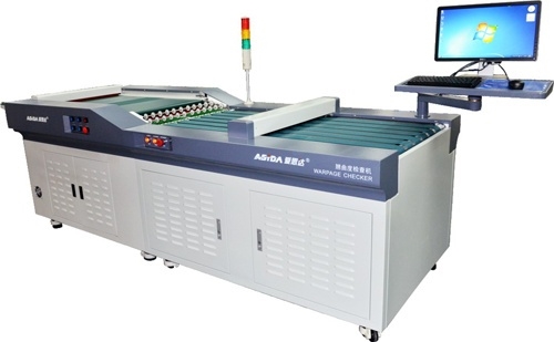
- Test Under Simulated Conditions: Use environmental testing chambers to simulate space conditions and validate material performance before finalizing your design.
- Consider Multilayer Designs: For complex systems, multilayer PCBs with mixed materials can balance thermal, electrical, and mechanical needs.
- Stay Updated on Standards: Adhere to industry standards like those from NASA or the European Space Agency (ESA) for material certification and testing.

Conclusion: Building Reliable PCBs for the Final Frontier
Designing PCBs for space probes is no small feat. The extreme conditions of space demand careful consideration of space-grade PCB laminate materials, precise PCB substrate selection for space probes, attention to outgassing PCB materials in space, and the right choice of high-frequency PCB materials for space applications. By understanding the challenges of temperature swings, radiation, vacuum conditions, and signal requirements, you can select materials that ensure reliability and performance over the long haul.
From polyimide laminates for thermal stability to PTFE composites for high-frequency signals, the right material can make or break a mission. Use the insights and tips in this guide to navigate the complexities of material selection and build PCBs that are ready to explore the unknown. With careful planning and the right resources, your designs can withstand the rigors of space and contribute to groundbreaking discoveries.