 ALLPCB


When it comes to ensuring the quality and reliability of printed circuit boards (PCBs), choosing the right inspection technique is crucial. Two common methods, microsectioning and X-ray inspection, offer distinct advantages and limitations. So, which one is better for your needs? In short, microsectioning is a destructive testing method ideal for detailed internal analysis, while X-ray inspection is a non-destructive approach perfect for examining hidden features without damaging the board. In this comprehensive guide, we’ll dive deep into the advantages and disadvantages of microsectioning, the limitations of X-ray inspection, and the broader context of destructive vs. non-destructive testing for PCBs. Let’s explore how to make an informed decision for your next project.
Understanding PCB Inspection: Why It Matters
In the world of electronics manufacturing, PCBs are the backbone of nearly every device. A single flaw in a PCB—whether it’s a poor solder joint, a misaligned via, or a hidden crack—can lead to catastrophic failure. Inspection techniques help identify these issues before they become costly problems. With the increasing complexity of modern PCBs, which often feature multiple layers and tiny components, selecting the right inspection method is more important than ever. Whether you’re dealing with high-density interconnects or intricate multilayer designs, understanding the strengths and weaknesses of microsectioning and X-ray inspection will ensure your boards meet the highest quality standards.
What Is Microsectioning? A Deep Dive into Destructive Testing
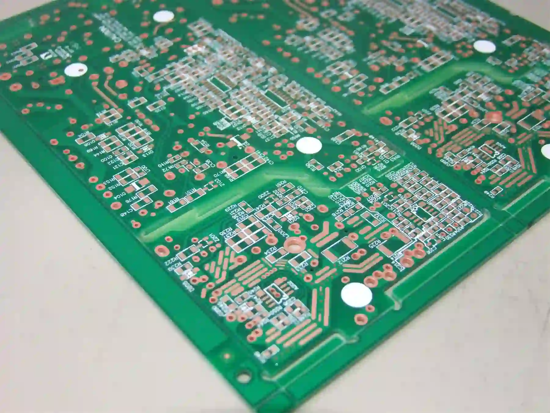
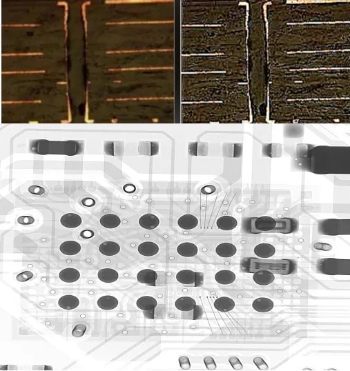
Microsectioning, also known as cross-sectioning, is a destructive testing method used to evaluate the internal structure of a PCB. This technique involves cutting a small section of the board, mounting it in a resin, polishing it, and examining it under a microscope. By physically dissecting the PCB, engineers can analyze details such as the thickness of copper layers, the quality of plated-through holes, and the integrity of solder joints.
Advantages of Microsectioning
- Highly Detailed Analysis: Microsectioning provides an unparalleled view of a PCB’s internal structure. Engineers can measure precise dimensions, such as copper thickness (often in the range of 1-2 oz per square foot, or approximately 35-70 micrometers), and identify microscopic defects like voids or delamination.
- Accurate Material Assessment: This method allows for a thorough examination of material properties, including the adhesion between layers and the quality of dielectric materials used in the PCB stack-up.
- Root Cause Identification: When a PCB fails, microsectioning can pinpoint the exact cause, whether it’s a manufacturing defect or a design flaw. For instance, it can reveal cracks in vias that might disrupt signal integrity at high frequencies (e.g., above 1 GHz).
Disadvantages of Microsectioning
- Destructive Nature: The most significant drawback of microsectioning is that it destroys the tested sample. Once a board is cut, it cannot be used again, making this method unsuitable for inspecting every unit in a production batch.
- Time-Consuming Process: Preparing a sample for microsectioning can take several hours, as it involves cutting, mounting, and polishing. This delays the inspection process, especially in high-volume manufacturing environments.
- Limited Scope: Since only a small section of the PCB is analyzed, defects in other areas of the board might go unnoticed. This method is best used as a spot-check rather than a comprehensive inspection tool.
What Is X-Ray Inspection? Exploring Non-Destructive Testing
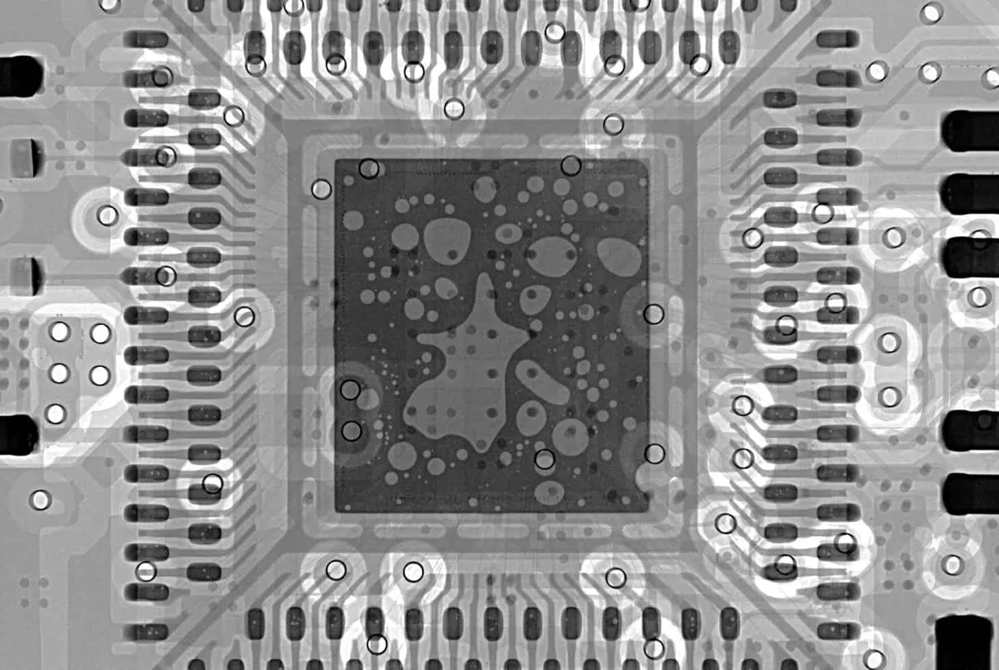
X-ray inspection is a non-destructive testing method that uses X-ray radiation to see inside a PCB without damaging it. This technique is particularly useful for examining hidden features, such as solder joints under ball grid array (BGA) components or internal traces in multilayer boards. By capturing detailed images of the board’s interior, X-ray inspection helps detect defects that are invisible to the naked eye.
Advantages of X-Ray Inspection
- Non-Destructive Testing: Unlike microsectioning, X-ray inspection preserves the PCB, allowing it to be used or further tested after inspection. This makes it ideal for high-value or production-ready boards.
- Comprehensive Coverage: X-ray systems can scan large areas of a PCB or even the entire board, identifying issues like misaligned components or hidden shorts across multiple layers.
- Speed and Efficiency: Modern X-ray inspection systems can produce results in minutes, making them suitable for high-throughput manufacturing environments where time is critical.
Limitations of X-Ray Inspection
- Limited Resolution for Fine Details: While X-ray inspection excels at detecting larger defects, it may struggle with microscopic issues, such as hairline cracks or voids smaller than 10 micrometers. This can be a problem for ultra-fine pitch components.
- Material Overlap Challenges: In densely populated PCBs, overlapping components or layers can obscure defects in X-ray images, making interpretation difficult. For example, a solder void under a BGA might be hidden by a nearby capacitor.
- Cost and Safety Concerns: X-ray equipment is expensive to purchase and maintain, often costing tens of thousands of dollars. Additionally, it requires strict safety protocols to protect operators from radiation exposure.
Destructive vs. Non-Destructive Testing for PCBs: A Broader Perspective
The choice between microsectioning and X-ray inspection often comes down to the fundamental difference between destructive and non-destructive testing methods. Let’s break down these approaches to understand their roles in PCB quality control.
Destructive Testing: When Precision Matters Most
Destructive testing, like microsectioning, sacrifices the sample to gain deep insights into its structure and quality. This approach is typically used during the design validation or failure analysis stages. For example, if a batch of PCBs fails during testing, engineers might use microsectioning to examine a few boards and identify manufacturing issues, such as inadequate plating in vias that could affect signal speeds (often measured in nanoseconds for high-speed designs). While destructive testing provides unmatched detail, its inability to preserve the board limits its use to specific scenarios.
Non-Destructive Testing: Preserving the Board for Production
Non-destructive testing, exemplified by X-ray inspection, prioritizes preserving the PCB for further use. This method is ideal for in-line quality checks during manufacturing, where inspecting every board—or at least a large sample—is necessary. Non-destructive methods can detect a wide range of defects without affecting the board’s functionality, making them suitable for final assembly checks. However, they may not offer the same level of detail as destructive methods, especially for internal material analysis.
Comparing Microsectioning and X-Ray Inspection: Key Factors to Consider
To choose the right inspection technique for your PCB project, consider the following factors:
- Stage of Development: If you’re in the early stages of design or conducting failure analysis, microsectioning’s detailed insights are invaluable. For production or final quality checks, X-ray inspection’s non-destructive nature is more practical.
- Type of Defects: Microsectioning excels at identifying microscopic internal defects, such as delamination or plating issues. X-ray inspection is better for detecting hidden solder joint problems or component misalignments in assembled boards.
- Budget and Time Constraints: Microsectioning is generally less expensive in terms of equipment but more time-intensive. X-ray inspection requires significant upfront investment but offers faster results, which can save time in large-scale production.
- Board Complexity: For multilayer PCBs with high component density, X-ray inspection can reveal hidden issues across the board. However, if you need to analyze the quality of specific layers or materials, microsectioning is the better choice.
Practical Applications: When to Use Each Method
Let’s look at some real-world scenarios to illustrate when to use microsectioning or X-ray inspection.
Scenario 1: Prototype Validation
During the development of a new PCB design for a high-speed communication device operating at 5 GHz, engineers notice inconsistent performance. To understand the root cause, they use microsectioning to examine the board’s internal structure. The analysis reveals uneven copper plating in vias, causing impedance mismatches (target impedance was 50 ohms, but measurements showed deviations up to 10 ohms). This destructive test provides the data needed to refine the manufacturing process.
Scenario 2: Production Quality Control
In a high-volume production run of consumer electronics, quality control teams need to ensure that every PCB meets standards without destroying valuable units. They implement X-ray inspection to check for solder joint integrity under BGA components. The process identifies a batch with 5% of boards showing voids in critical joints, allowing the team to address the issue without scrapping entire lots.
Combining Techniques for Optimal Results
In many cases, the best approach is to combine microsectioning and X-ray inspection to leverage their complementary strengths. For instance, during the initial stages of a project, microsectioning can be used on a few prototype boards to validate the design and manufacturing process. Once production begins, X-ray inspection can ensure consistent quality across all units. This hybrid strategy balances the need for detailed analysis with the practical demands of large-scale manufacturing.
Conclusion: Making the Right Choice for Your PCB Inspection Needs
Choosing between microsectioning and X-ray inspection depends on your specific goals, budget, and production stage. Microsectioning offers unmatched detail for failure analysis and design validation but destroys the board in the process. On the other hand, X-ray inspection provides a non-destructive way to examine hidden features, though it comes with limitations in resolution and cost. By understanding the advantages and disadvantages of microsectioning, the limitations of X-ray inspection, and the broader context of destructive vs. non-destructive testing for PCBs, you can make an informed decision that ensures the quality and reliability of your products.
At ALLPCB, we’re committed to supporting your journey with high-quality manufacturing and inspection solutions tailored to your needs. Whether you require in-depth analysis or efficient production checks, our expertise can help you achieve flawless results. Explore our services to see how we can elevate your next PCB project.


