ALLPCB


Are you new to PCB design and looking to create a board for an AI accelerator? This guide will walk you through the essentials of designing AI accelerator PCBs using a popular online design platform. Whether you're focusing on high-speed processing or power efficiency, we'll cover the basics of PCB design, specific considerations for AI hardware, and step-by-step instructions to build your first board. Let’s dive into this beginner-friendly tutorial on crafting open-source PCB layouts for cutting-edge AI applications.
Why Design PCBs for AI Accelerators?
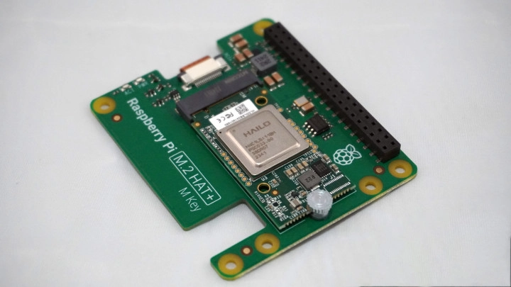
AI accelerators are specialized hardware designed to handle the intense computational demands of artificial intelligence tasks, such as machine learning and neural network processing. These devices require custom PCBs to manage high-speed signals, power delivery, and thermal performance. Designing a PCB for an AI accelerator can seem daunting, but with the right tools and knowledge, even beginners can create efficient and reliable boards. Using an online design tool simplifies the process, making it accessible to hobbyists and professionals alike.
In this guide, we’ll focus on the unique challenges of AI accelerator design, including signal integrity and power management, while providing practical tips for beginners. By the end, you’ll have a clear understanding of how to start your project with confidence.
What Makes AI Accelerator PCBs Unique?
Before we get into the design process, it’s important to understand what sets AI accelerator PCBs apart from standard circuit boards. These boards are built to support high-performance chips like GPUs, TPUs, or custom ASICs, which process massive amounts of data in parallel. Here are some key factors that make these designs unique:
- High-Speed Signals: AI accelerators often operate at frequencies above 1 GHz, requiring careful routing to avoid signal loss or interference. For example, differential pairs must maintain impedance values around 100 ohms for optimal performance.
- Power Delivery: These chips draw significant current, sometimes exceeding 100 watts. A robust power distribution network (PDN) is essential to maintain stable voltage levels, often around 0.9V to 1.2V for core components.
- Thermal Management: High power consumption leads to heat generation, so PCBs must include thermal vias and heat sinks to dissipate heat effectively.
- Dense Component Layout: AI accelerators pack many components into a small area, requiring multi-layer boards (often 6 to 12 layers) to accommodate complex routing.
Understanding these requirements will guide your design decisions as you create a PCB tailored for AI workloads.
Getting Started with Online PCB Design Tools
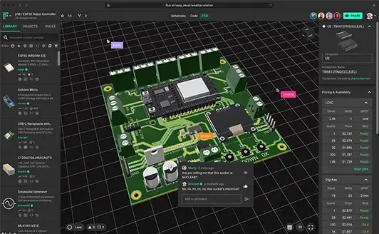
For beginners, online PCB design tools are a fantastic way to start. These platforms offer user-friendly interfaces, extensive component libraries, and often integrate with manufacturing services for seamless production. They are especially helpful for open-source PCB projects, as many tools allow you to share designs with the community or access pre-made templates.
Most online tools provide features like schematic capture, PCB layout editors, and simulation capabilities. This means you can design, test, and finalize your AI accelerator board without installing complex software. Plus, many platforms are free or low-cost for basic use, making them ideal for beginners.
Step-by-Step Guide to Designing an AI Accelerator PCB
Now, let’s walk through the process of designing a PCB for an AI accelerator. This tutorial assumes you’re using a web-based design platform and have a basic understanding of electronics. If you’re completely new to PCBs, don’t worry—we’ll keep things simple and actionable.
Step 1: Define Your Project Requirements
Start by outlining the specifications for your AI accelerator board. Ask yourself what kind of performance you need. For example:
- Will it support a specific chip, like a neural processing unit (NPU) or FPGA?
- What are the power requirements (e.g., 12V input, 1.0V core voltage)?
- How many I/O connections are needed for data transfer (e.g., PCIe lanes or DDR memory interfaces)?
Write down these details to create a clear roadmap for your design. For a beginner project, consider starting with a small-scale accelerator using an off-the-shelf development board as a reference.
Step 2: Create a Schematic Diagram
The schematic is the blueprint of your PCB. It shows how components like the AI chip, power regulators, and connectors are wired together. In your online design tool, start a new project and add components from the library. Focus on these key elements for an AI accelerator:
- Main Processor: Place the AI chip at the center of your design. Ensure you match its pinout with the datasheet specifications.
- Power Supply: Add voltage regulators to step down input power to the required levels (e.g., 1.2V for core, 3.3V for I/O). Include decoupling capacitors (typically 0.1μF to 10μF) near the chip to stabilize voltage.
- Memory Interfaces: Connect high-speed memory like DDR4 using controlled impedance traces to maintain signal integrity.
- Connectors: Add interfaces like USB or PCIe for data input and output.
Double-check connections to avoid errors before moving to the layout stage.
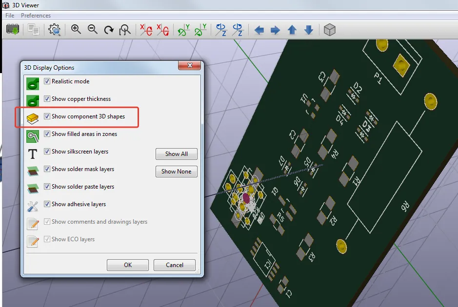
Step 3: Design the PCB Layout
Once your schematic is ready, switch to the PCB layout editor in your design tool. This step involves placing components on the board and routing traces to connect them. Follow these tips for an AI accelerator design:
- Component Placement: Position the AI chip centrally to minimize trace lengths for high-speed signals. Place power components nearby to reduce voltage drops.
- Layer Stackup: Use a multi-layer board (e.g., 6 layers) with dedicated ground and power planes. This helps with noise reduction and signal integrity. A typical stackup might include signal layers on top and bottom, with ground and power in the middle.
- Trace Routing: Route high-speed signals (like DDR or PCIe) as differential pairs with consistent spacing to maintain impedance (e.g., 100 ohms). Keep traces short and avoid sharp bends—use 45-degree angles instead of 90-degree turns.
- Thermal Design: Add thermal vias under the AI chip to transfer heat to a ground plane. Plan for a heat sink if the chip dissipates more than 50 watts.
Take your time with routing, as mistakes here can lead to signal issues or board failure.
Step 4: Validate Your Design
Most online design tools include design rule checks (DRC) to catch errors like unconnected pins or overlapping traces. Run a DRC to ensure your board meets manufacturing standards. Additionally, simulate power delivery and signal integrity if your tool supports it. For instance, check if voltage drops across power traces are within 5% of the target (e.g., no more than 0.06V drop for a 1.2V supply).
If you’re unsure about a specific aspect, consult online forums or open-source PCB communities for feedback. Sharing your design for review can catch issues you might have missed.
Step 5: Export and Manufacture
After validating your design, export the Gerber files, which are the standard format for PCB manufacturing. Many online design platforms integrate with fabrication services, allowing you to upload files directly and order prototypes. For an AI accelerator PCB, choose a manufacturer that supports multi-layer boards and tight tolerances (e.g., trace widths down to 5 mils).
Start with a small batch of 1-5 boards to test your design before scaling up. This minimizes costs if revisions are needed.
Tips for Beginner PCB Designers Working on AI Accelerators
Designing a PCB for an AI accelerator is a complex task, but these tips can help beginners succeed:
- Start Simple: Begin with a basic design using a reference board or open-source project as a template. Gradually add complexity as you gain experience.
- Focus on Signal Integrity: High-speed signals are prone to interference. Use ground planes and keep traces short to minimize noise.
- Plan for Power: Underestimating power needs can lead to board failure. Use online calculators to estimate current draw and trace width (e.g., a 10-mil trace can carry about 1A safely).
- Leverage Community Resources: Open-source PCB communities offer free designs, tutorials, and advice. Use these to learn best practices and avoid common mistakes.
- Test Thoroughly: Once your board is manufactured, test it with low-power conditions first to avoid damaging components. Gradually increase load while monitoring temperature and voltage.
Common Challenges and How to Overcome Them
As a beginner, you’ll likely face hurdles while designing an AI accelerator PCB. Here are some common issues and solutions:
- Signal Crosstalk: High-speed traces can interfere with each other. Solution: Increase spacing between traces or use shielding with ground vias.
- Power Instability: Voltage drops can cause the AI chip to malfunction. Solution: Add more decoupling capacitors (e.g., 10μF near power pins) and widen power traces.
- Thermal Overload: Excessive heat can degrade performance. Solution: Incorporate thermal vias and ensure airflow around the board during operation.
- Layout Errors: Misplaced components can lead to routing issues. Solution: Use the auto-placement feature in your design tool as a starting point, then manually adjust for optimization.
Patience and attention to detail will help you navigate these challenges over time.
Conclusion: Start Your AI Accelerator PCB Journey Today
Designing a PCB for an AI accelerator may seem intimidating, but with the right approach and tools, it’s an achievable goal for beginners. By using an online design platform, you can create professional-grade boards without needing expensive software or years of experience. Focus on understanding the unique needs of AI hardware—high-speed signals, robust power delivery, and thermal management—and follow the step-by-step process outlined above.
Remember, every expert started as a beginner. Take advantage of open-source PCB resources, experiment with small projects, and learn from each design iteration. With practice, you’ll be crafting cutting-edge boards for AI accelerators that power the future of technology. Get started today and bring your ideas to life!